Unpack and verify contents against the BOM — 51 components total across the 3-deck PCB stack.
Sort resistors and capacitors by value before touching the iron. Six tantalum capacitors require careful polarity check.
Confirm tools: temperature-controlled iron (25–40 W, fine tip, 680 °F), 0.7–1.0 mm solder, multimeter (volts, continuity, diode test), heat-shrink, anti-static mat.
Read this entire guide and the Errata section before placing a single component.
⚠️ Counterfeit 2N3819
Widespread on eBay and unauthorized marketplaces. Fakes test as NPN BJTs, not JFETs. Order only from Mouser, Newark, Small Bear, or NTE Parts Direct — and test every unit with a transistor tester before installation.
⚠️ ESD-sensitive devices
Transistors and JFETs are sensitive to electrostatic discharge. Use an anti-static wrist strap or mat. Handle the 2N3819 by the body, not the leads. Never connect or disconnect the microphone with phantom power active.
⚠️ Nitrile gloves required for the Top PCB
The high-impedance front-end (1 GΩ R1, 100 MΩ R3, 220 MΩ R2, 68 MΩ R4/R5) is acutely sensitive to finger oils. Gloves on throughout Step 3.
▶ 💡 Materials checklist (per kit)
Parts & kits: D-U47fet Round Microphone PCB, U47fet Component Kit, Styroflex Capacitor Kit (18 pF, 33 pF), D-U47fet body, capsule mount (threaded sleeve / spacer), capsule (M7 or K47), audio transformer (09331 or equivalent).
Tools: 25–40 W iron with fine tip, flux + 0.7–1.0 mm solder, side cutters, tweezers, needle files, multimeter, heat-shrink tubing + sleeving + cable ties, small Phillips screwdrivers, medium thread locker, anti-static mat / wrist strap.
02
Inspect PCBs
Lay all boards on a clean, static-safe surface. Identify each: Top, Middle, Bottom, and Switch sub-PCB.
Sort components by value — resistors and caps separated and labelled before you start. Six tantalum capacitors will need polarity verification.
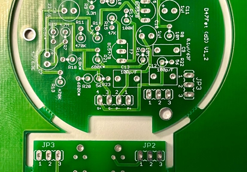
Identify the JP1 (capsule LC), JP2 (OUT), JP4 (transformer), and the dual headers (JP1/JP2 deck connection) on the silkscreen.
Warm up the iron to 680 °F. Verify the tip is clean and at temperature.
⚠️ The 3-deck assembly order matters
Build the boards in the order in this guide: Top PCB high-impedance components first (most ESD-sensitive), then tantalums, then the switch sub-PCB inserted between Top and Middle, then Middle and Bottom. Do NOT solder the switch sub-PCB headers to the Middle PCB until the stack is dry-fit and aligned (Step 5).
03
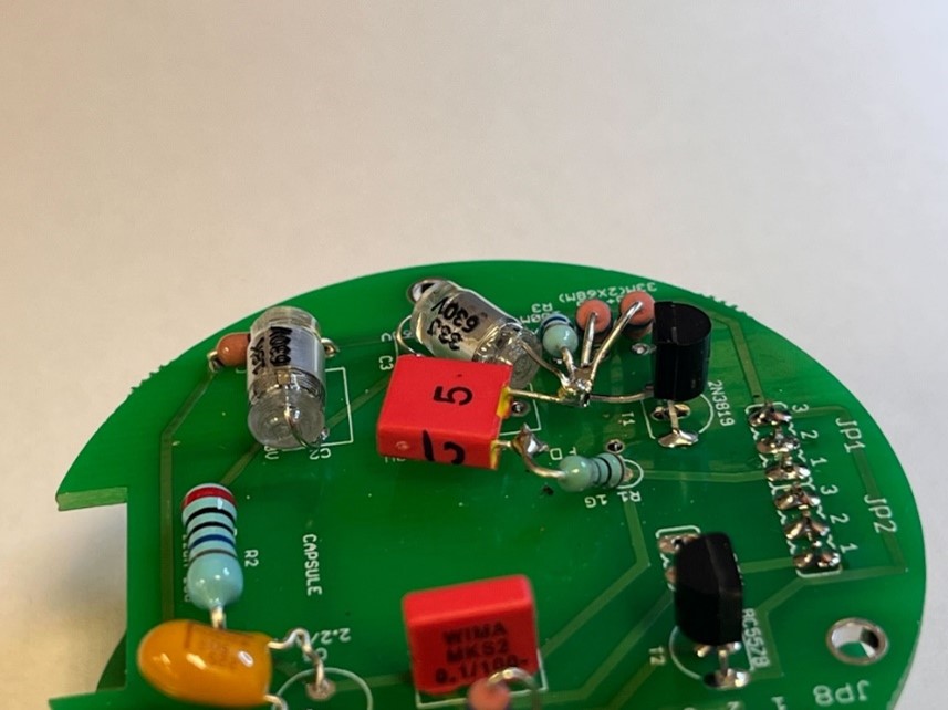
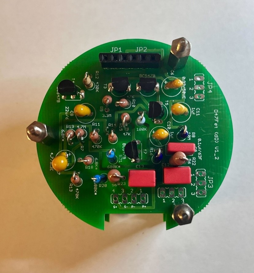
Top PCB — High-Impedance Components
Top PCB populated with high-impedance components. The JFET gate pin is lifted free of the board; the 1 GΩ polarisation resistor and 68 MΩ low-pass resistors connect directly to the floating gate node. Keep leads short and flat; use minimal solder.
Lift the 2N3819 gate pin (middle pin) upward so it floats above the PCB. Trim short.
Low-pass resistors 68 MΩ (R5+ & R5) — install near the lifted FET gate pin.
Pad −10 dB resistor R3 (100 MΩ) and C3 (33 pF polystyrene) connect to the lifted gate pin.
C1 2200 pF — first pin connects to the lifted gate pin.
Capsule polarisation resistor R1 (1 GΩ) with C1 (2200 pF).
Install the 6-pin header with the longer pin facing backward.
⚠️ Nitrile gloves required throughout this entire step
Finger oils on the high-impedance area create irreversible leakage paths that permanently degrade self-noise. Do not touch the 1 GΩ resistor leads, their pads, or the surrounding PCB with bare hands — not even before soldering.
⚠️ ESD precaution
Transistors and MOSFETs are sensitive to electrostatic discharge. Handle the 2N3819 by the body, never by the leads. Use an anti-static wrist strap.
▶ 💡 Polystyrene capacitor handling (C3, C2)
Polystyrene caps (18 pF C2, 33 pF C3) are heat-sensitive. Use a thermal-mass clip on the lead between the cap body and PCB. Solder from the underside. Excessive heat can damage the dielectric and cause years-later failures (silent or popping). Never apply IPA or acetone near polystyrene caps once installed — both attack the dielectric.
▶ 💡 Cleaning the high-impedance area after soldering
Clean both sides of the Top PCB with 91 % or higher IPA on a clean toothbrush — 30–60 seconds per side. Air-dry several minutes before powering up. Documented cases of noisy builds were resolved by this cleaning alone, no component replacement needed.
04
Top PCB — Tantalum Polarity
Six tantalums on this PCB. Solder one lead, verify orientation, then commit the second. The brown-bar end is +.Reference: brown bar on the capacitor body = + (positive) lead. Match to the + pad on the silkscreen.
Identify the PCB + pad — silkscreen marking adjacent to the round through-hole.
Align tantalum + lead to the + pad. The + side of the cap is marked with a brown bar or + sign.
Solder one lead first; verify orientation visually; then solder the other lead.
Install the 6-pin header with the longer pin facing backward.
⚠️ Reversed tantalum = damage on first power-up
Tantalum capacitors fail catastrophically (often shorted, sometimes flaming) when reversed. Triple-check polarity on each of the six tantalums. Solder one lead, inspect, then commit the second.
▶ 💡 Don't overheat the capacitor
Tantalums tolerate brief soldering heat but degrade with prolonged contact. Use the iron at 680 °F, touch the pad for 2–3 seconds, withdraw. If the joint isn't clean, remove the part and try again rather than reheating in place.
05
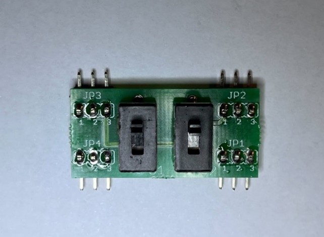
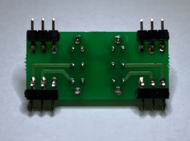
Switch PCB Assembly
Switch sub-PCB front: two slide switches and four 3-pin headers. Labels JP1–JP4 visible on the silkscreen.Switch sub-PCB solder side — avoid excess solder; clean joints only.Middle PCB underside. Do not solder the switch headers to the Middle PCB — this allows the Top PCB to be removed later.
Install 2× slide switches. Solder the middle pin first for alignment; verify the switch sits flat and square; then solder the remaining pins.
Install 4× 3-pin headers per the silkscreen layout.
⚠️ Do NOT solder the headers to the Middle PCB
Assemble the headers while inserting the switch PCB between the Middle and Top PCBs — this aligns the three-board stack precisely. Leaving the headers unsoldered to the Middle PCB allows the Top PCB to be removed later for service.
⚠️ Slider switches are fragile during disassembly
If you ever remove the PCB stack from the body, support the switches by hand. In previous builds, some have broken from excessive force during removal.
▶ 💡 EG2205 switch obsolescence (Errata E3)
The original switch part (EG2205) has gone obsolete with some suppliers. Current production kits ship a verified-equivalent slide switch from MicrophoneDIY. If you sourced your own switches and the footprint differs slightly, verify against the photos before mounting.
06
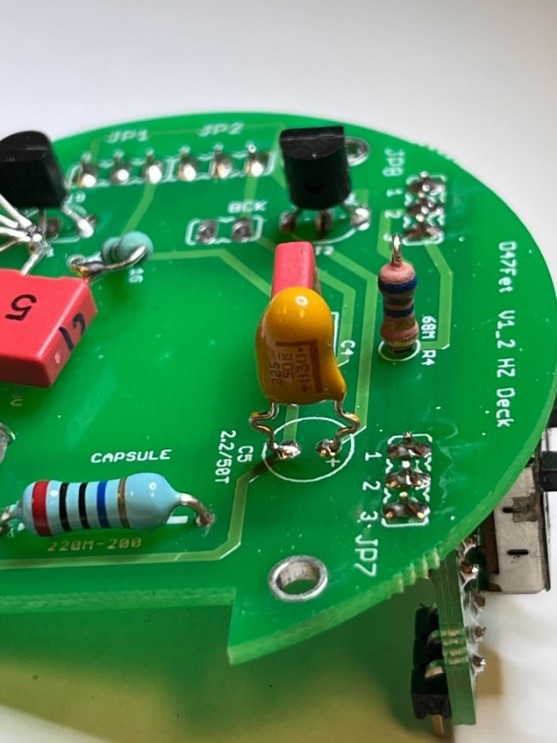
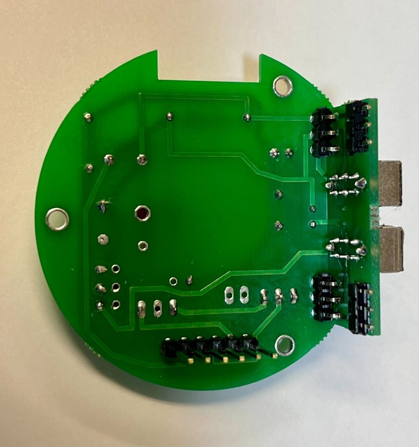
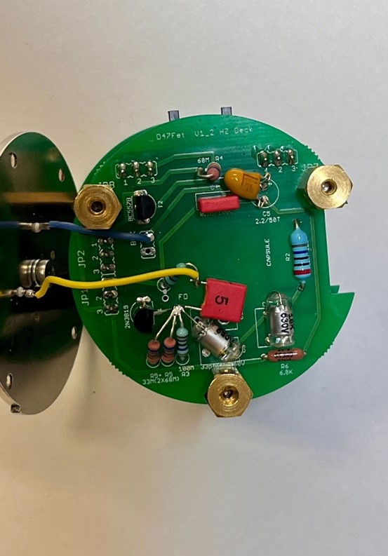
Middle PCB Assembly
Middle PCB with all components populated. JP1 header pins install straight, facing up. Verify tantalum polarity on each capacitor before soldering.
Install all components in the order: lowest-profile first (resistors), then film capacitors, then tantalums, then transistors, then headers.
JP1 header pins straight, facing up. These mate with the dual-header connector to the Bottom PCB.
Verify tantalum polarity on every tantalum cap before soldering.
Set the soldering iron at 680 °F. Clean the tip frequently to prevent buildup.
▶ 💡 BJT transistor identification
T3, T4, T6, T7 are BC547B (NPN, 45 V, 100 mA). T2 and T5 are BC557BTF (PNP). Don't mix them up — orientation matters. The flat side of the transistor case faces the silkscreen flat-side indicator.
07
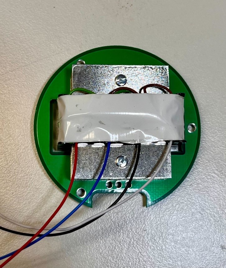
Bottom PCB & Output Transformer
Transformer mounted to the Bottom PCB. Nylon washers prevent shorts between the transformer body and PCB traces. Lock washers prevent loosening. Tighten evenly — snug only.
Mount the transformer with screws and lock washers. Add nylon washers between the transformer body and PCB to prevent any winding from shorting to a solder pad.
Verify primary / secondary orientation against the BOM and the wiring section (Step 8) BEFORE soldering. The 09331 ratio is 9:1 step-down.
Tighten the mounting screws evenly. Snug only — over-torque can crack the transformer bobbin or the PCB.
⚠️ DCR-test before soldering, always
Higher-resistance pair = primary (capsule side, P+/P−); lower-resistance = secondary (XLR side, S+/S−). Expect approximately 80–100× ratio for a 9:1 step-down. Color codes are NOT standardized across transformer manufacturers — verify by DCR.
▶ 💡 Transformer alternatives
The canonical choice is the 09331 (Cinemag CM-13101 reproduction) with 9:1 ratio. AMI T49 is also documented and supported. Beware of similar-looking transformers with different ratios — a 6.5:1 unit installed in this 9:1 circuit will produce low output and altered tone (see FAQ on 3U Audio GZT-47).
08
Wiring (Transformer + XLR)
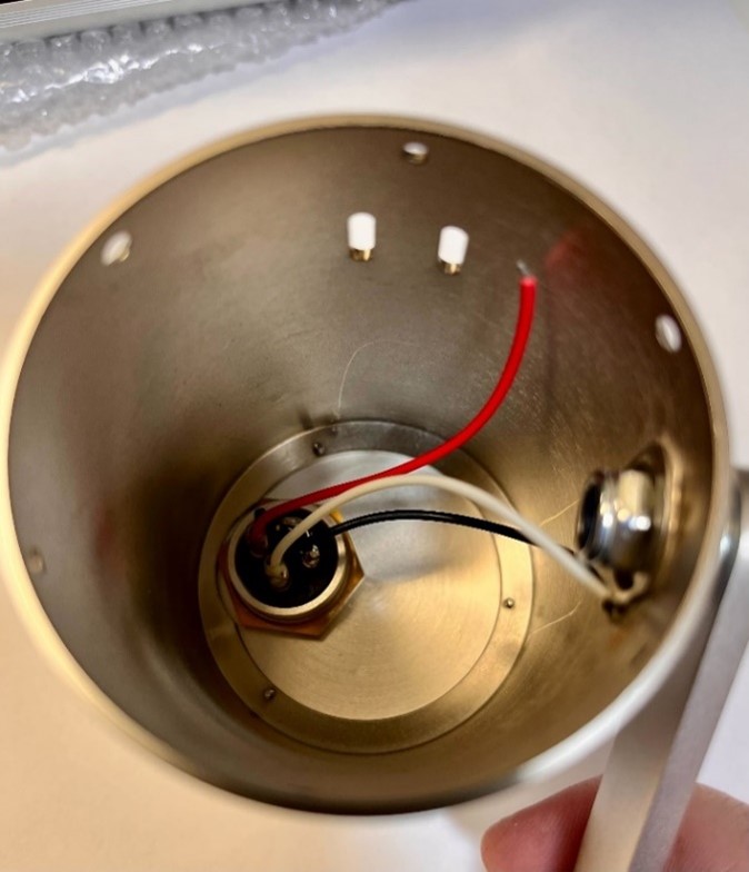
XLR connector in the body. Tip: extend the wires a few inches to give yourself slack when inserting the PCB stack.PCB connector view (P+, P−, S+, S− pads). Verify the color-to-pad mapping against the table below before soldering.
Pin 1 → Black (Shield / GND)
Pin 2 → Red (Hot +)
Pin 3 → White (Cold −)
Apply heat-shrink to every individual lead at the connector end.
Extend wires by a few inches to make PCB installation easier — they can be trimmed later if too long.
Never float the transformer shield. Shield/case wires always tie to XLR Pin 1.
⚠️ Errata E1 (Round-only) — XLR pin 1 needs a dedicated chassis-ground wire
On the 3-deck stack, a single XLR mounting screw is not enough to ground the entire body chassis reliably. Run a dedicated wire from XLR pin 1 to a PCB standoff or chassis lug. Without it: hum that disappears when you touch the body.
▶ 💡 AMI T49 transformer wiring (Errata E4 from square-thread)
If you're using an AMI T49 transformer instead of 09331, note that some AMI shipments arrived with a wiring sticker that is reversed relative to the canonical labeling (Errata E6 from the square thread). Always DCR-test before soldering: higher resistance pair → primary (P+/P−), lower → secondary (S+/S−).
09
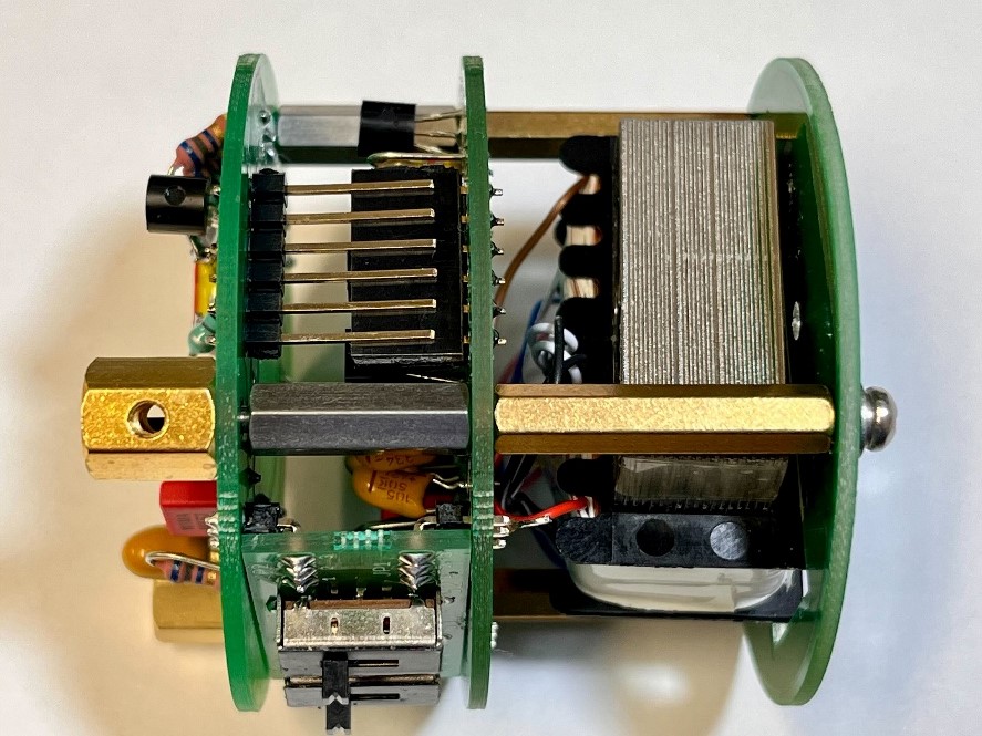
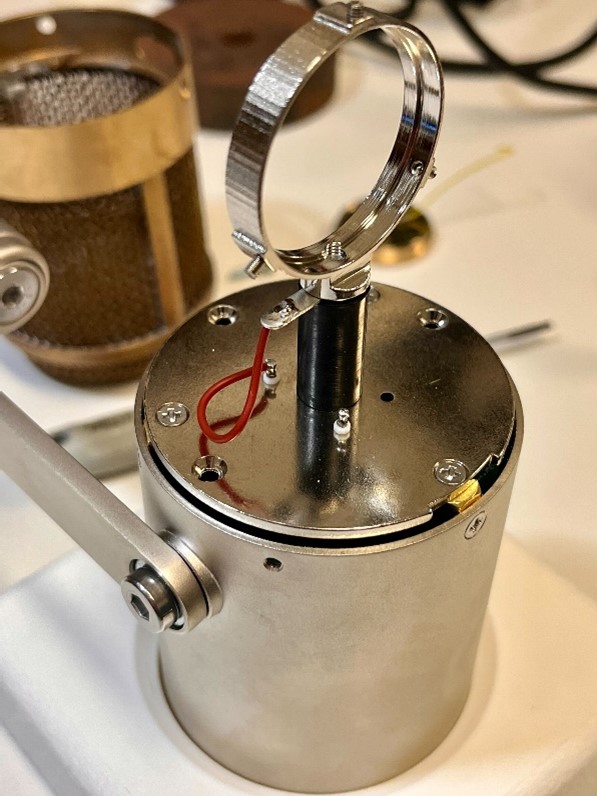
PCB Standoff Assembly
Stack and secure the three PCBs with M2.5 standoffs. Alignment is critical — the side M2.5 hole must be tangent to the PCB edge to fit inside the body.
Start from the Top PCB.
Install M2.5 × 9.5 mm and M2.5 × 16 mm standoffs.
Add a lock washer to bring the total spacing to 16.7 mm.
Verify the side M2.5 hole is tangent to the PCB edge — this alignment is critical to fit the assembly inside the microphone body.
Secure the Middle PCB on top using M2.5 × 25 mm standoffs threaded into the 16 mm standoffs below.
Ensure the Switch PCB and 6-pin header are correctly inserted between the Top and Middle PCBs before tightening.
This prevents the misalignment that occurred in early builds.
Install the Bottom PCB and secure with M2.5 screws + lock washers.
⚠️ Errata E2 (Round-only) — Top hex spacer can short the Hi-Z trace
Some early Round PCB revisions had insufficient clearance between the M2.5 spacer and the high-impedance trace on the Top PCB underside. Inspect for proximity; if the spacer touches the trace, add an insulating washer (Kapton or fiber).
▶ 💡 If the boards bind during stack-up
Loosen all screws, realign by sight, and retighten gradually in a star pattern. Do not overtighten — snug is enough. The stack must be free of mechanical pre-stress before the body slides on.
10
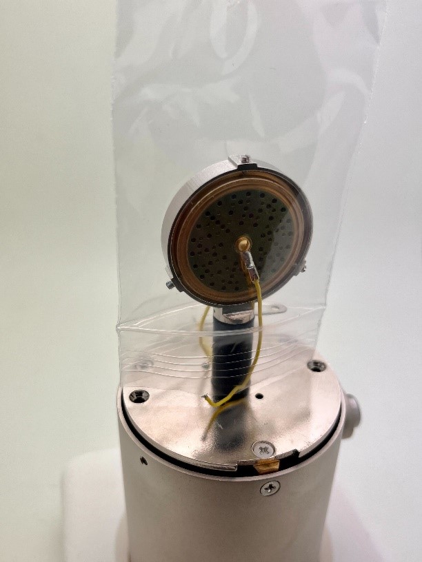
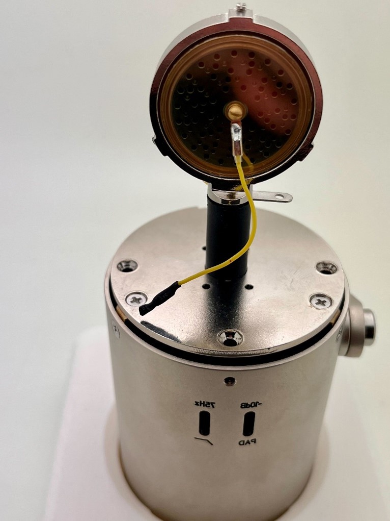
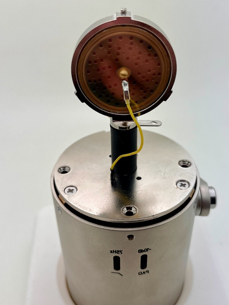
Capsule Mounting
Capsule plate with Teflon pin installed. Yellow = front diaphragm (Hi-Z gate node). Blue = rear (heat-shrunk and routed into the hole).Capsule positioned above the body. Handle by the rim only — never touch the diaphragm surface.
Cover the capsule with the zip bag before soldering the wire to the Teflon pin. Flux spatter on the diaphragm is permanently damaging.
Mount the capsule with the marked side facing front — this orientation has been chosen for best performance in the D-U47FET.Rear capsule view. Rear diaphragm wire is isolated with heat-shrink, then inserted into the hole in the metal plate — do not leave it floating.
Install the Teflon pin into the top metal board. This is the floating gate node — keep it clean.
Handle the capsule with the nitrile gloves provided. By the rim only — never touch the diaphragm.
Fit the capsule into the mount. Mark on the front for the D-U47FET (chosen for best performance).
When soldering the capsule wire to the Teflon pin, cover the capsule with the small zip bag to prevent flux or solder residue from reaching the diaphragm.
Slide heat-shrink tubing over the rear capsule wire. Apply heat from the opposite side, keeping it away from the capsule.
Insert the heat-shrunk wire into the empty hole of the metal plate.
⚠️ Most delicate step of the entire build
It is easy to slip the screwdriver and scratch the diaphragm — this destroys the capsule. Take your time. Use a small flat screwdriver. Tighten gently. The diaphragm is sensitive to finger oils, dust, flux residue, and any direct contact.
⚠️ Avoid overheating the Teflon pin
When unsoldering the existing wire beneath the Teflon pin, work fast — Teflon deforms when overheated and can lose its insulating geometry.
11
Final Assembly & First Test
Pre-power inspection: all solder joints clean and shiny, no solder bridges, tantalum polarities verified, transformer DCR sane, XLR pin 2–3 reads ~30 Ω (not zero), pin-1 ground continuity confirmed (Errata E1 fix in place).
Insert the PCB stack into the body. Align the switches against the body cutouts.
Connect to a 48 V phantom-powered preamp at low gain. Power up.
Test all switches for proper operation: pad and pattern (or whichever your assembled variant has).
Listen for self-noise. Hum that disappears when touching the body chassis = Faraday-cage failure (check the XLR pin-1 ground wire).
⚠️ Switches feel tight on first body insertion — this is normal
They must fit precisely into the body slots. If you ever disassemble later, handle the switches carefully — in previous builds, some have broken due to excessive force during removal.
⚠️ PCB compression / overtightening can ruin the sound
The D-47FET contains extremely high-impedance circuitry. Mechanical pressure alone can alter the circuit even without a visible short. If the Top Hi-Z PCB is tightened until it makes direct contact with metal standoffs or brass nuts, the microphone may sound thin, distorted, or unstable — and lose low-frequency response. Maintain a visible gap between the Hi-Z PCB and metal hardware. Use the supplied lock washers and insulating spacers; do not compress the stack tightly. Verify the sound after final tightening.
⚠️ Final noise tests require the body fully assembled
The microphone body and headbasket act as a Faraday cage. Testing with the body or grille removed may produce audible 50/60 Hz hum — the enclosure provides essential electrostatic and magnetic shielding. Do not panic if "naked" tests show hum.
▶ 💡 Troubleshooting checklist
No output at all: Verify phantom voltage at the XLR (~48 V DC pin 2 to 1, pin 3 to 1). Check transformer DCR (primary & secondary). Check for cold solder joints — set the iron to 680 °F, touch each suspect joint for 3–4 seconds.
Hum that disappears when touching the body: Faraday-cage failure. Verify the XLR pin-1 chassis-ground wire (Errata E1).
Output but very low: Re-verify transformer wiring (P/S not reversed) and DCR. If using AMI T49, check that the wiring sticker isn't reversed (Errata E4 / E6 from square-thread).
Crackle / pops at rest: High-impedance contamination on the Top PCB. Re-clean with 91 % IPA on a soft toothbrush. Inspect for cold joints around R1, R2, R3, R5.
▶ 💡 Storage
Store the assembled microphone in a wooden mic case or padded box. Dust and moisture both degrade self-noise over time. The high-impedance front-end is particularly sensitive to humidity.
Stuck?
Common questions — distilled from years of community builds
Before posting on the forum, search here first. These answers were extracted from years of community discussion across the Round and Square D-47FET threads — the most common problems, solved.
🔍
No matching questions — try a different search term or clear the filter.
Circuit Reference
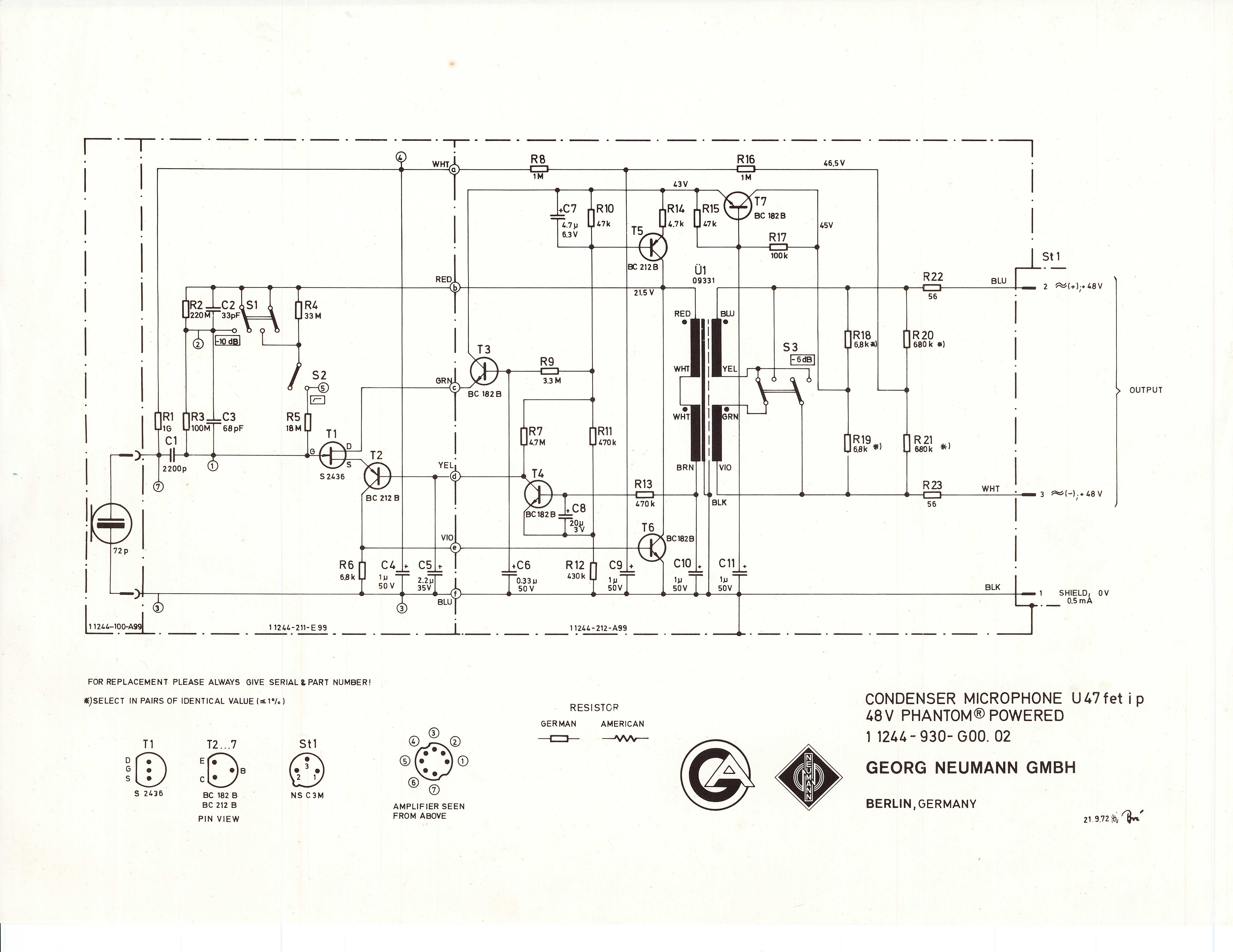
Full circuit schematic — click to zoom. Key nodes: JFET gate (Hi-Z floating input), BJT complementary buffer, R1 1 GΩ capsule polarisation, phantom regulator (+48 V → regulated supply), 9:1 step-down output transformer to XLR.
Key nodes: 2N3819 drain = main signal output node into the BJT stage; BJT pair (BC547B / BC557BTF) = complementary buffer; R1 1 GΩ = capsule polarisation; Transformer P/S = 9:1 step-down to XLR; phantom = 48 V at the input.
Component List
37 line items · 51 components · rev 1R0
#
Ref
Qty
Value
Description
Part Number
Type
Errata
Known issues — read before you build
ID
Severity
Affects
Description
E1
Critical
Round PCB only
XLR pin 1 needs a dedicated chassis-ground wire. The 3-deck stack is not adequately grounded by the single XLR mounting screw alone. Run a dedicated wire from XLR pin 1 to a PCB standoff or chassis lug. Symptom without this fix: hum that disappears when you touch the body.
E2
Critical
Round PCB early revisions
Top hex spacer can short the high-impedance trace. Insufficient clearance between the M2.5 spacer and the Hi-Z trace on the Top PCB underside. Inspect during stack assembly; if the spacer contacts the trace, add an insulating washer (Kapton or fiber).
E3
Warning
Round PCB
EG2205 slide switch obsolescence. The original switch part has gone end-of-life with several suppliers. Current MicrophoneDIY kits ship a verified equivalent. If you sourced your own, verify the footprint before mounting.
E4
Critical
AMI T49 transformer (square & round)
Some AMI T49 shipments have a reversed wiring sticker. Documented across several builds in the square-thread era. Always DCR-test before soldering: higher-resistance pair = primary (P+/P−); lower-resistance = secondary (S+/S−). Expect roughly 80–100× ratio for 9:1.
E5
Critical
Square PCB only
R6 trimmer was removed from the BOM. The original PCB shipped with a trimmer at R6; it has been removed. Jumper the potentiometer pad contact and use R6 = 6.8 kΩ fixed (not 3.6 kΩ).
E6
Warning
All variants
Counterfeit 2N3819. Widespread on eBay and unauthorized marketplaces. Fakes test as NPN BJTs with base / collector / emitter pinout, not JFETs. Source only from Mouser, Newark, Small Bear, or NTE Parts Direct. Test every unit with a transistor tester before installation.
E7
Warning
All variants — high-impedance area
HZ turret install requires gloves and IPA cleaning. Finger oils on the high-impedance area create irreversible leakage paths. Use nitrile gloves throughout the Top PCB assembly and clean with 91 %+ IPA after soldering. Documented as the #1 cause of self-noise issues in finished builds.
E8
Warning
Round PCB — body fitment
ShuaiYin body mounting-arm screw can loosen over time. Reported on the round-PCB thread by multiple builders. Apply a drop of medium thread locker to the mounting-arm thread; verify periodically.
Reference Gallery
Additional build photos — click to zoom
▶Show all reference photos— photos
Ready to build?
The complete kit — body, PCB, components, capsule, transformer — configurable at microphonediy.com.