Step-by-step assembly for the D-U67 — a faithful recreation of the Neumann U67 tube condenser circuit. EF86 pentode, K67 capsule, external PSU. Synthesized from the official assembly guide and community builds.
01
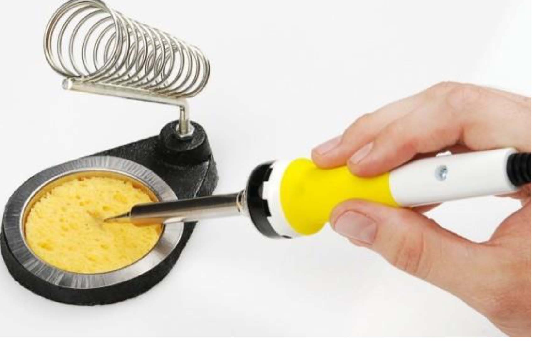
Tools & Safety
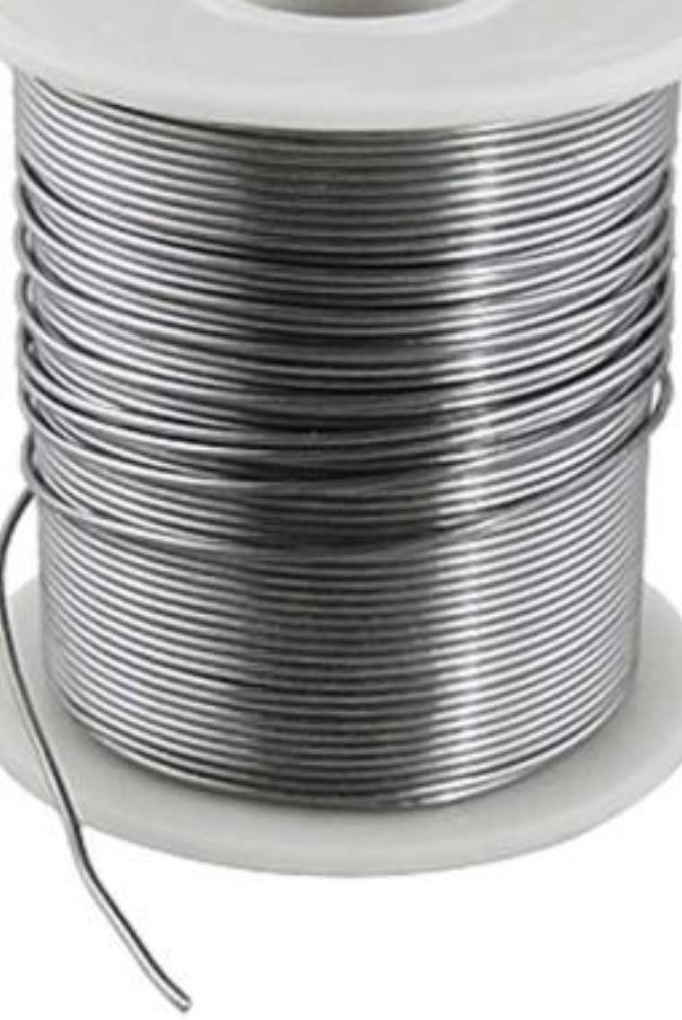
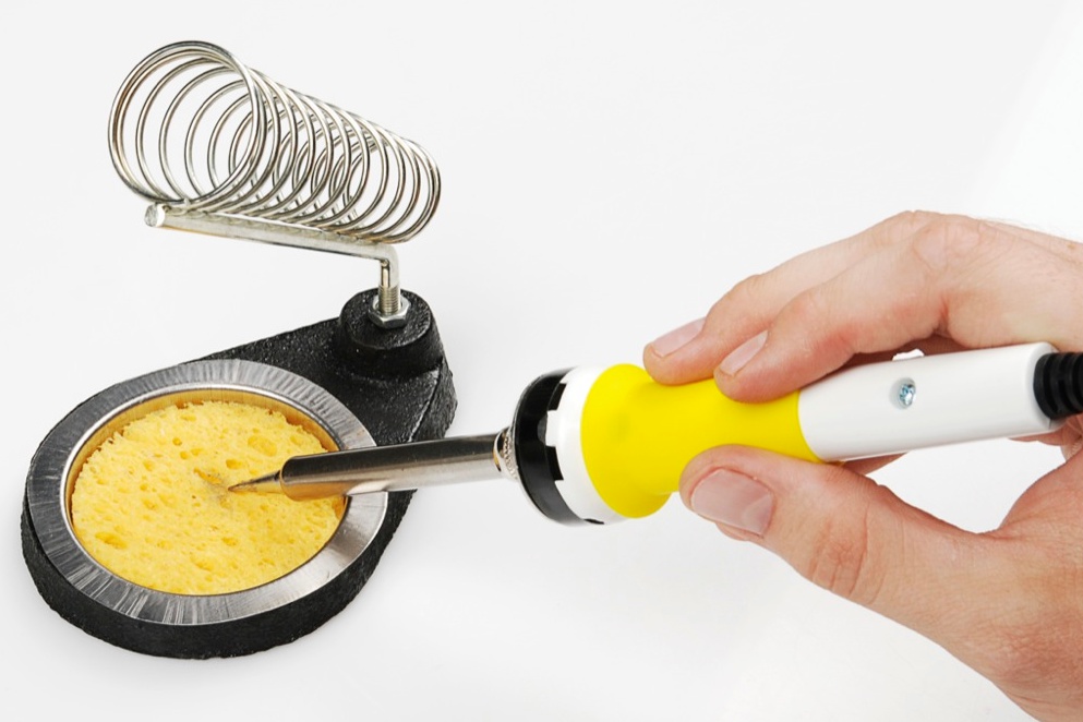
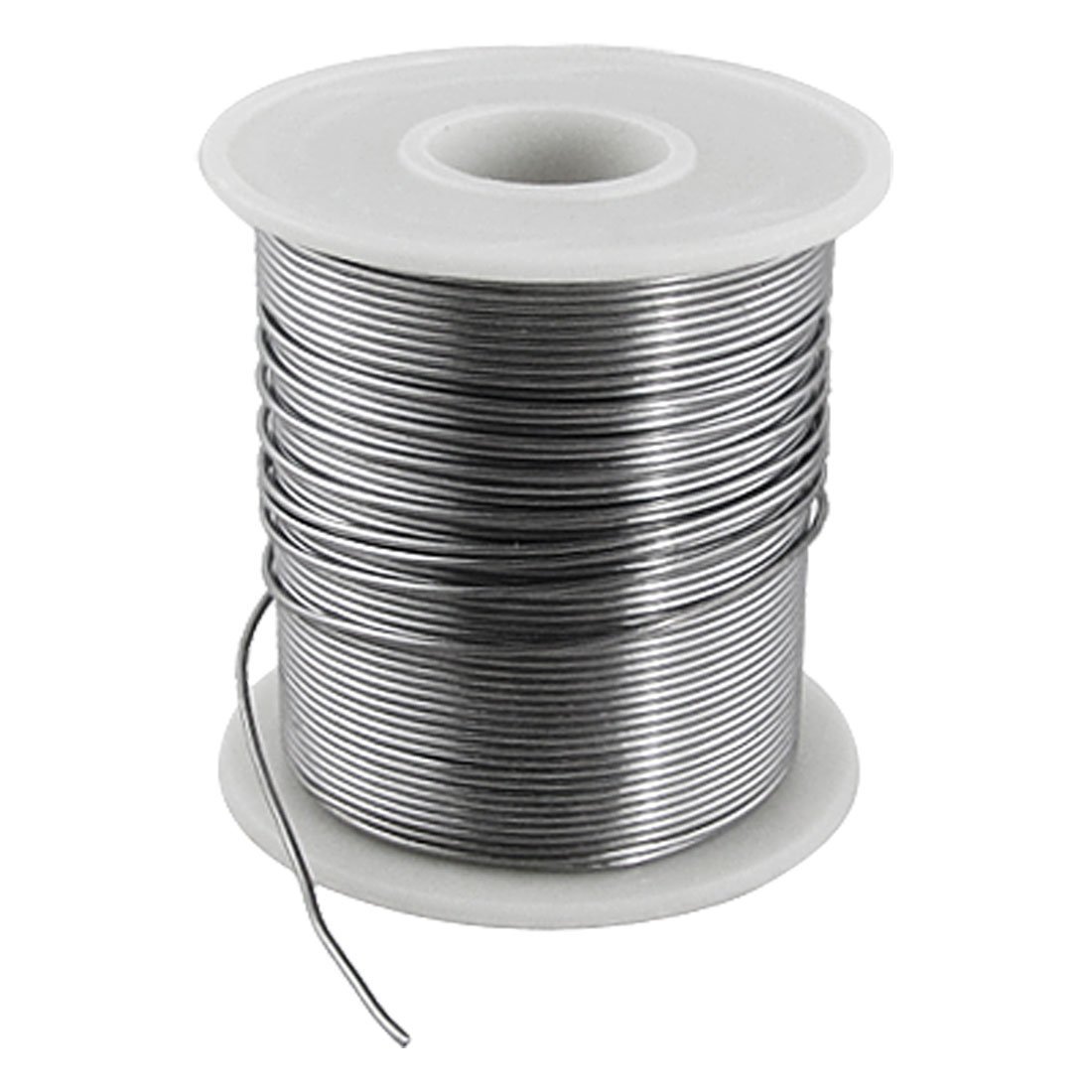
Temperature-controlled iron — fine tip, ~350 °C0.6–0.8 mm rosin-core solder
Soldering iron: temperature-controlled, 25–40 W, fine tip, ~350 °C / 660 °F.
Solder: 0.6–0.8 mm rosin-core. Cleaning: 91 % IPA + acid brush. Multimeter required for voltage checks.
Alligator-clip heat sink required for all polystyrene (styroflex) capacitors — C10 and C17.
Read this entire guide before placing any component.
⚠️ High-impedance components — nitrile gloves required
R1E and R8E (400 MΩ) and R9, R2E, R16E (68 MΩ) must be handled with nitrile gloves. Install these last, after all other components are soldered and the PCB is clean. Finger oils on leads or solder joints permanently degrade noise performance.
02
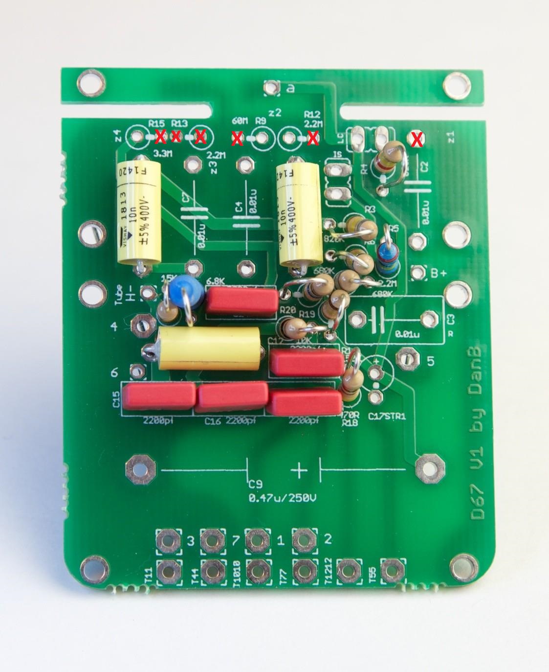
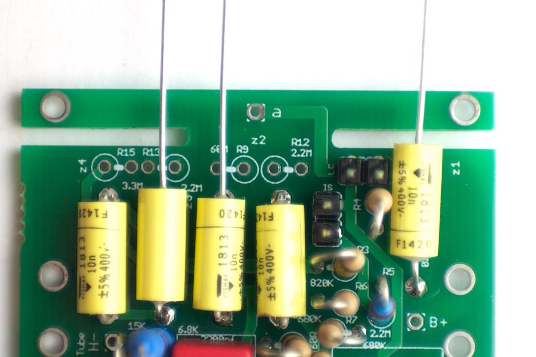
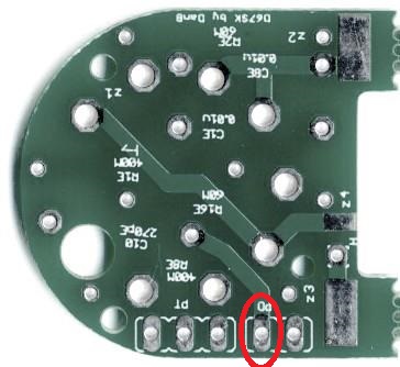
Populate Main PCB
Main PCB — component sideInstall these parts firstSolder side — bend leads to hold parts before soldering
⚠️ Do NOT install these parts yet: R15, R13, R9, R12, C7, C4, C2, C17
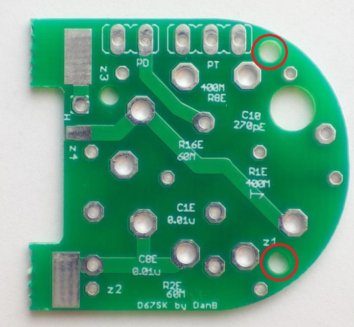
These components are installed in later steps using specific forming and routing techniques. Installing them now will block access or require rework. Also do not use any holes marked with a red ✕ on the PCB.
Install all remaining parts shown on this page. Stuff all components at once, bending leads on the bottom so they hold in place without taping — ensure no bent lead overlaps another trace.
Clip all leads flush, then solder. Inspect each joint.
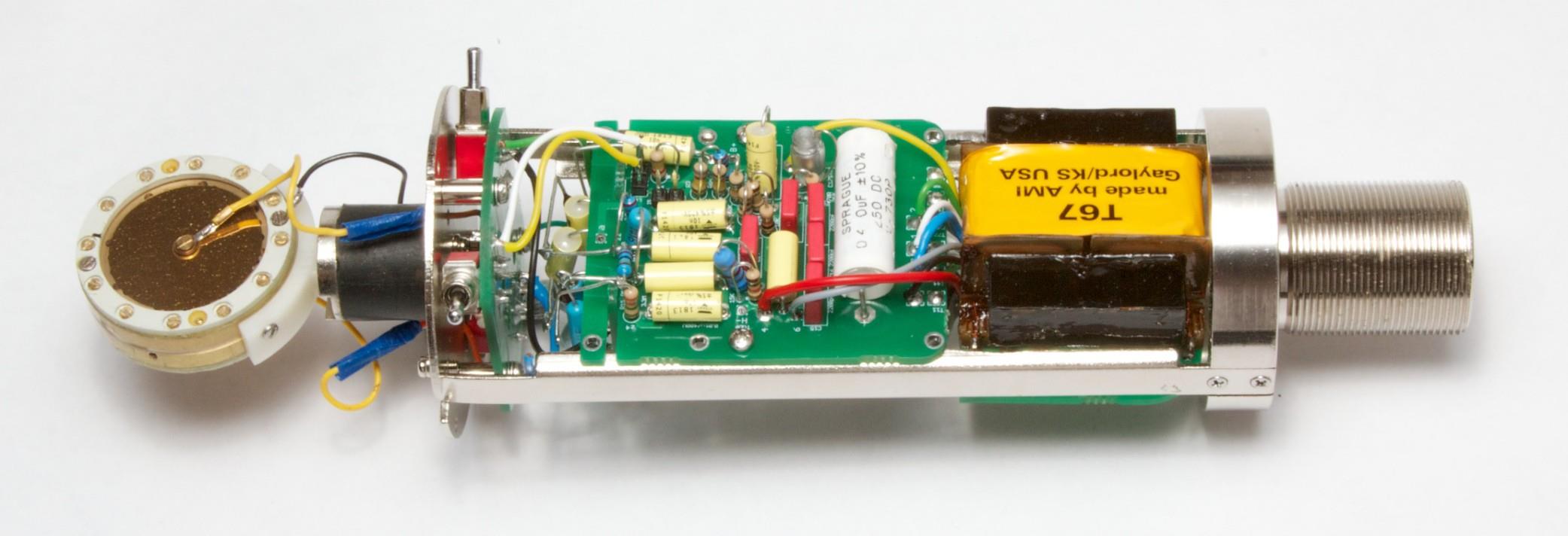
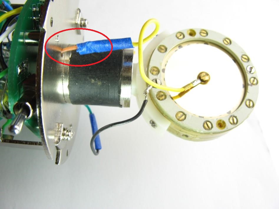
The D-U67 uses two PCBs: the main PCB (this guide) and the tube PCB (Steps 9–21), connected via PT and PD Molex headers.
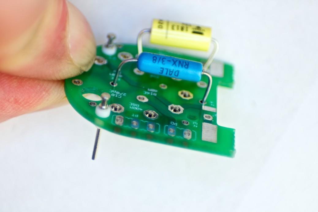
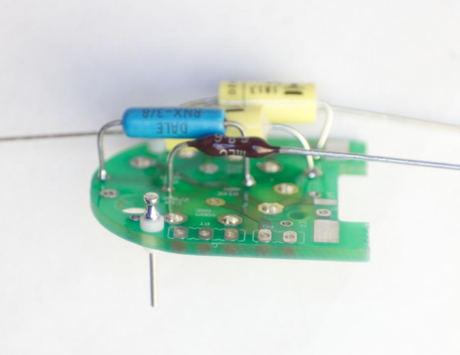
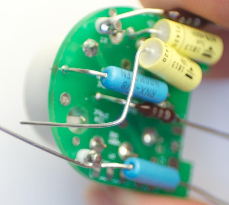
03
Install C4 & C7
C7 installed on main PCBC4 installed on main PCB
Install C4 and C7 flush to the PCB.
These are part of the coupling and bypass network on the main PCB.
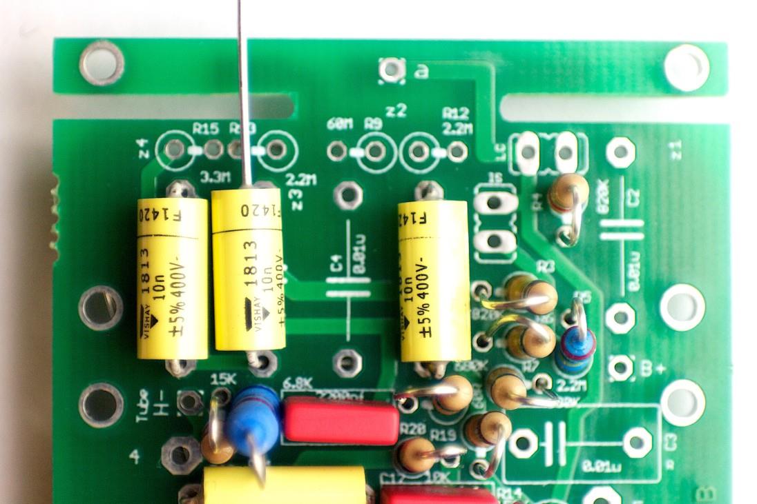
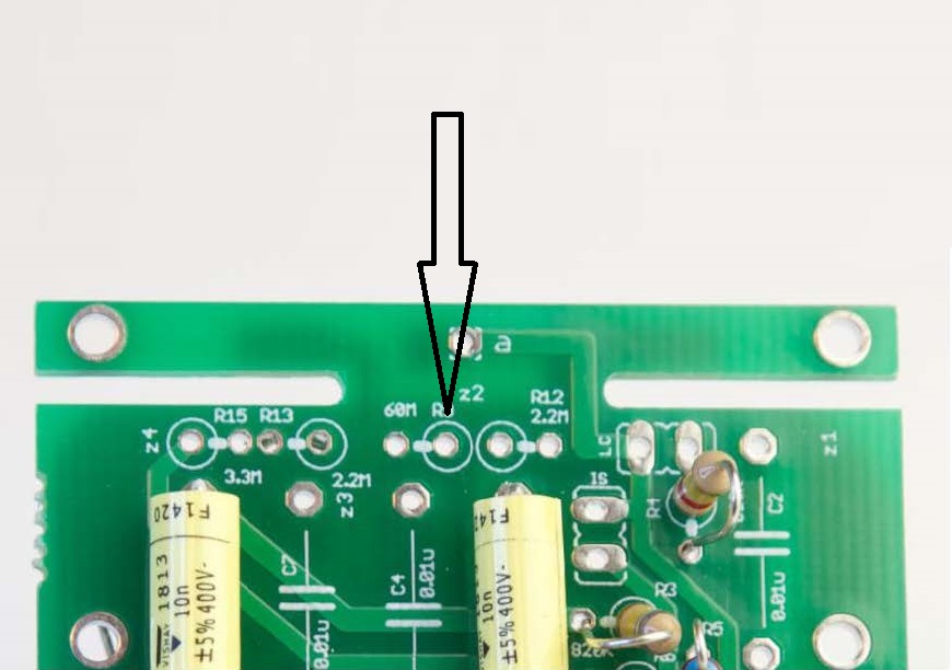
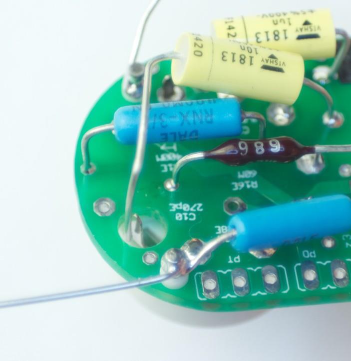
04
Install C2, R13 & R15
C2 installedR13 and R15 positioned
Install C2, and R15 per board silkscreen. C2 and R15 are not yet soldered in final position — they will be formed and soldered in the next steps.
Verify resistor values with a multimeter before installing.
05
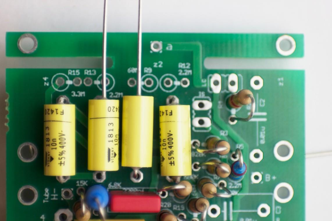
Bend & Trim R13
Bend R13 lead to shapeTrim R13 lead to length
Bend R13 lead to the shape shown — it will bridge between two board points off-pad.
Trim lead length to match the target position in Step 6.
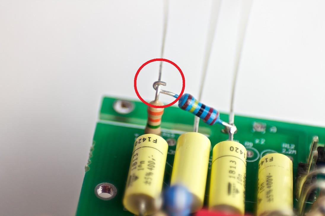
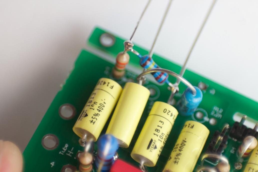
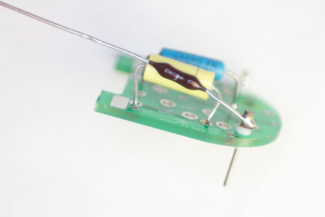
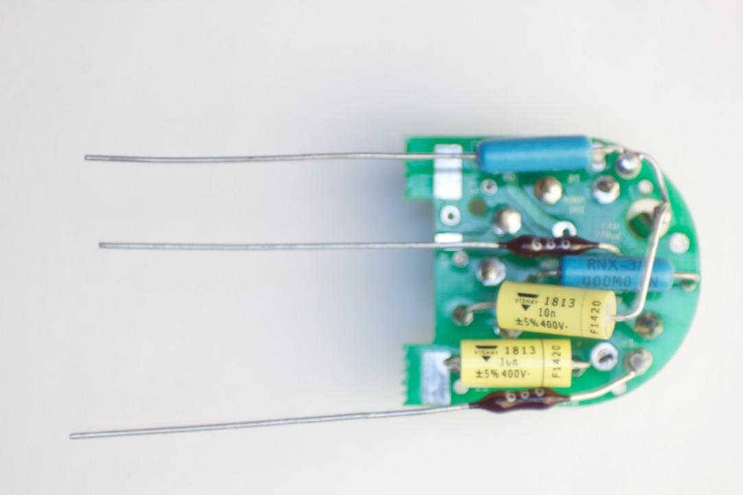
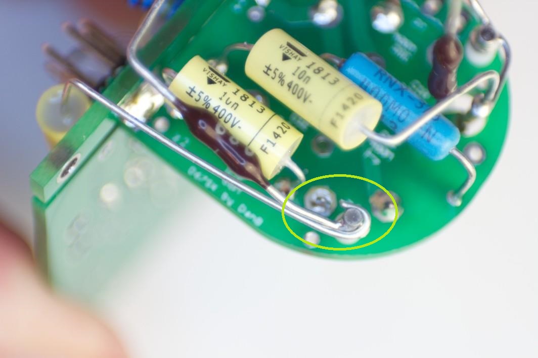
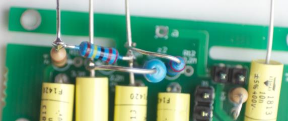
06
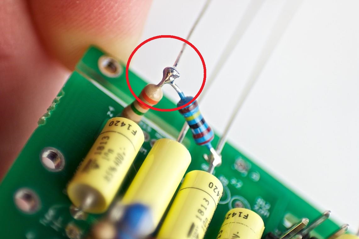
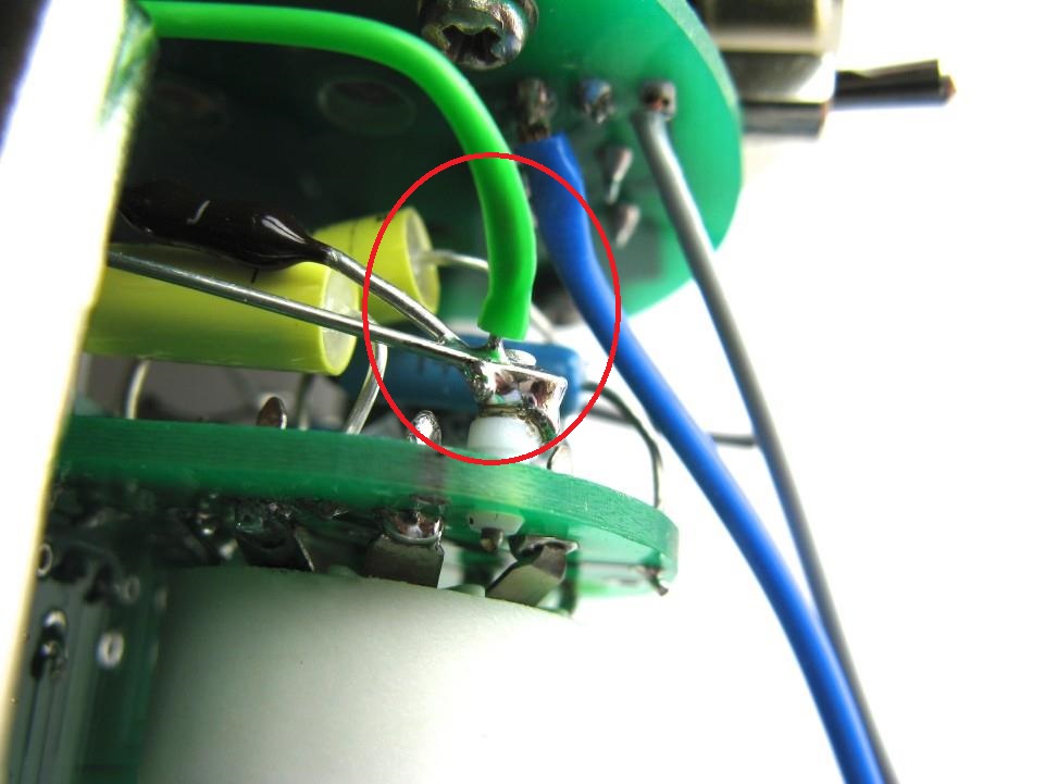
Solder R13/R15 to C4; Install R9
R13 soldered to C4 leadR15 connection pointR9 installed
Solder the bent R13 lead to the C4 lead and R15 as shown — this is an off-PCB solder joint, not a through-hole pad.
Install R9 (68 MΩ — high-Z, nitrile gloves). Do not touch leads with bare hands.
⚠️ R9 is 68 MΩ — high-impedance handling required
Wear nitrile gloves when handling R9. Keep the lead and joint area clean of flux residue — clean with IPA after soldering.
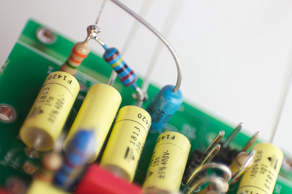
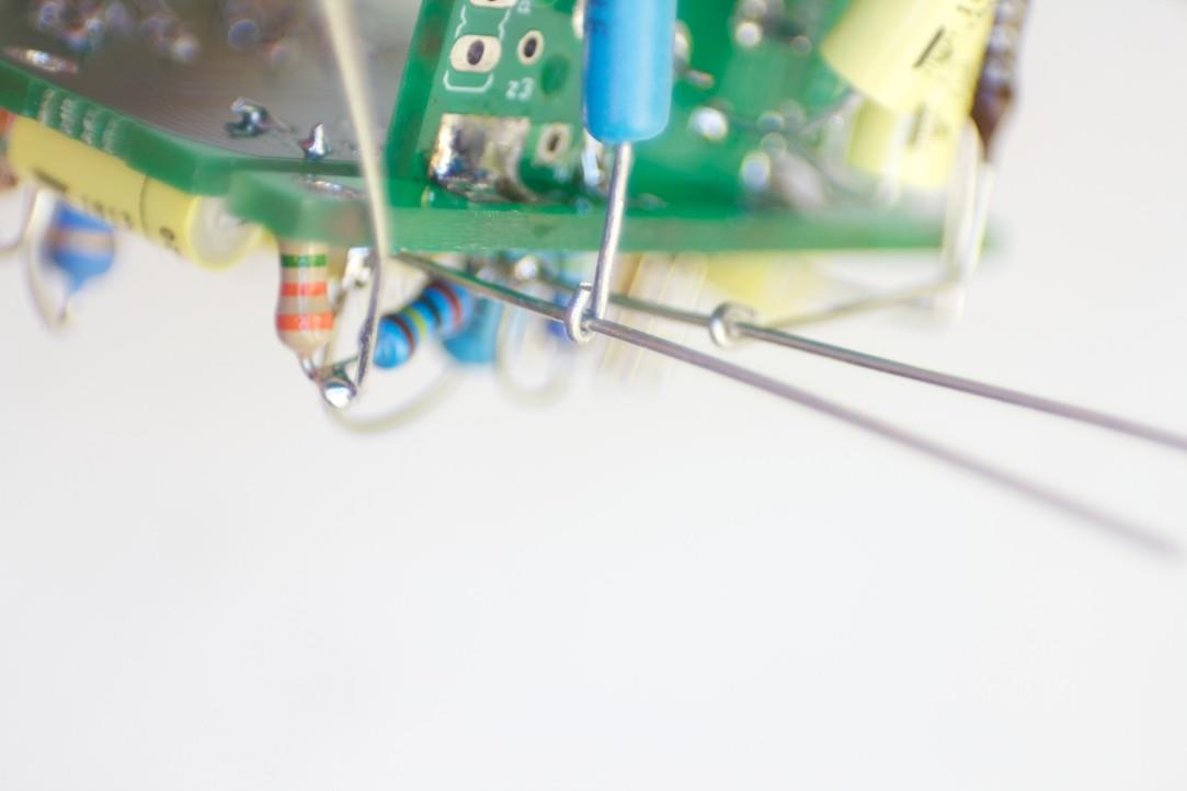
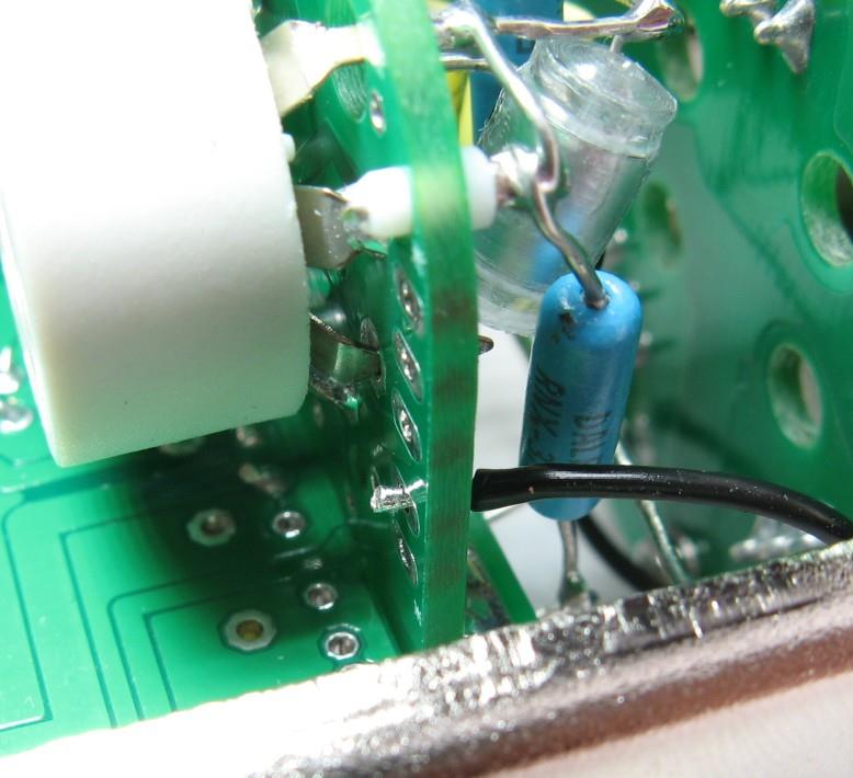
07
Form R9 Hook to C7
Form hook at R9 endHook end to C7 lead, then solder
Form a small hook at the free end of R9 using round-nose pliers.
Hook over the C7 lead and solder. Nitrile gloves on throughout.
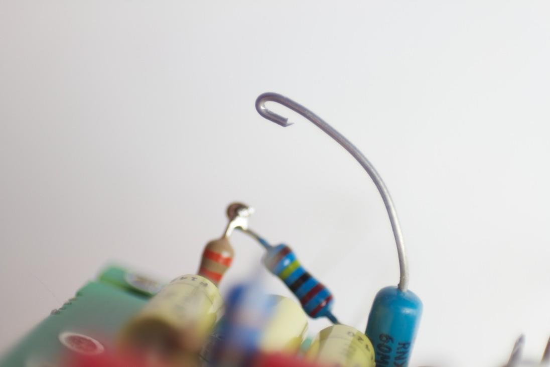
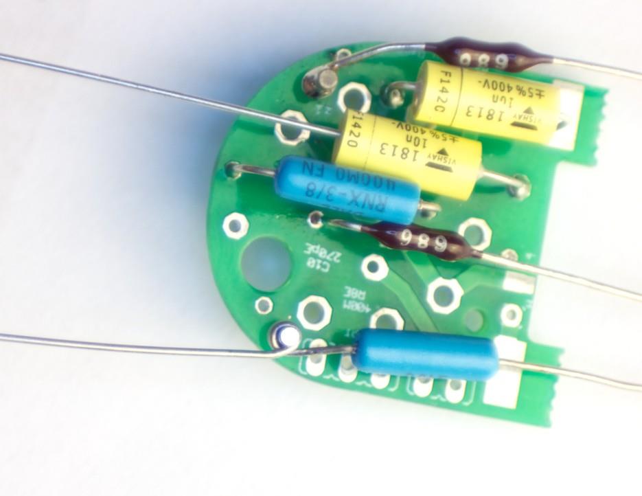
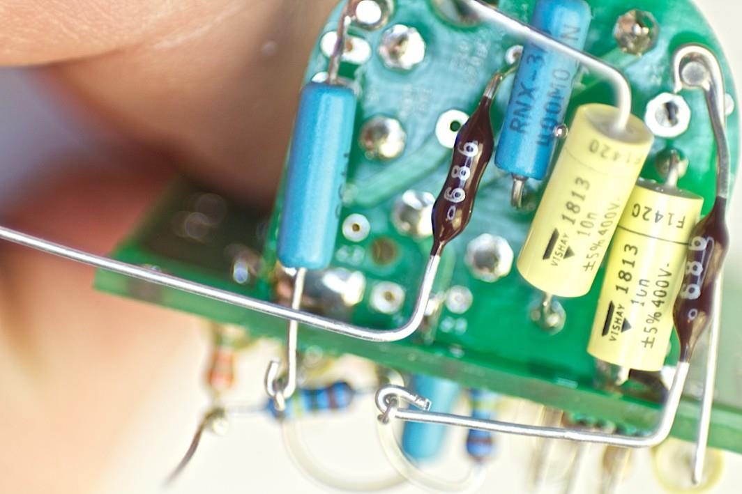
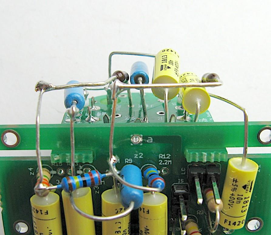
08
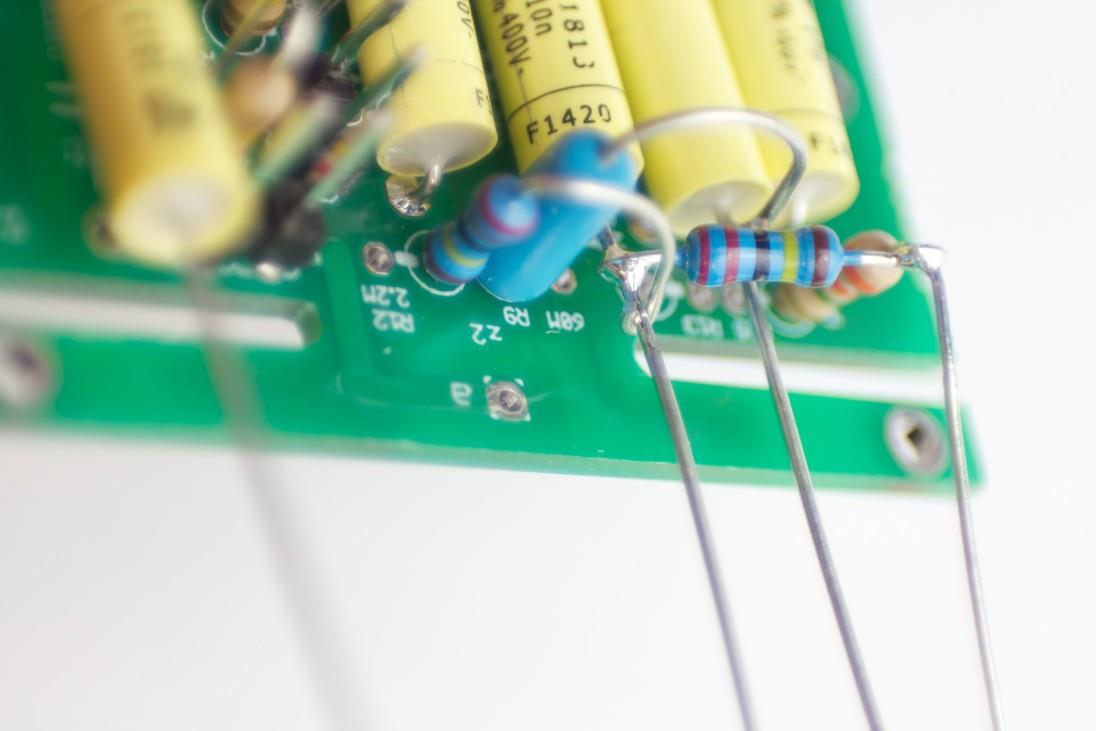
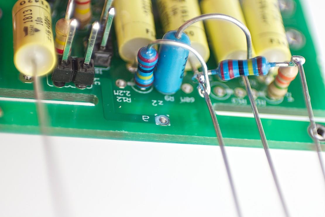
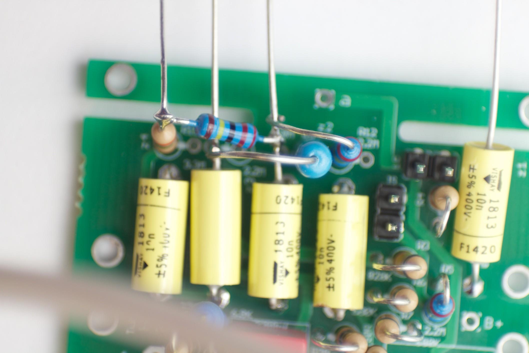
Install R12
Form R12 — same technique as R9Route R12 to C4 positionR12 soldered — completed
Apply the same forming and hook technique used for R9. R12 solders to the C4 lead position.
R12 is 2.2 MΩ — standard handling. Verify the solder joint is bright and smooth.
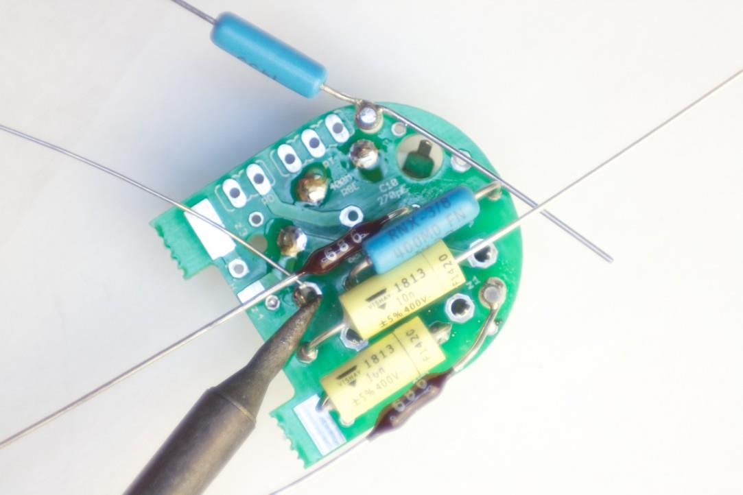
09
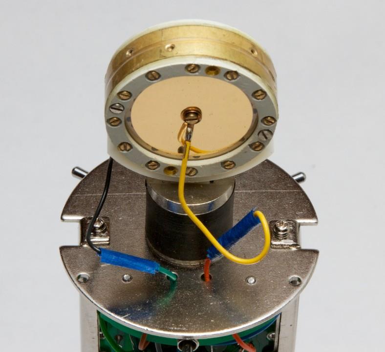
Tube PCB Component Map
Tube PCB component placement — study before populating
Study this reference drawing before placing any component on the tube PCB.
Identify positions: C1, C8, R1, R2, R8, R16, tube socket, and the PT/PD Molex header pads.
The tube PCB carries the EF86 pentode and its bias network. It connects to the main PCB via the PT and PD headers.
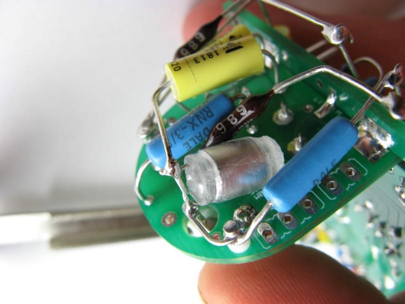
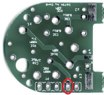
10
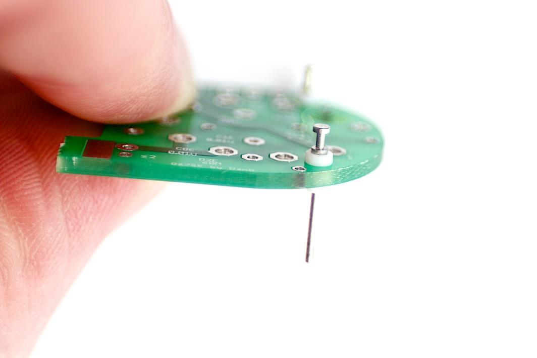
Install Tube PCB Turrets
Turret 1 — seat flush to PCB surfaceBoth turrets installed
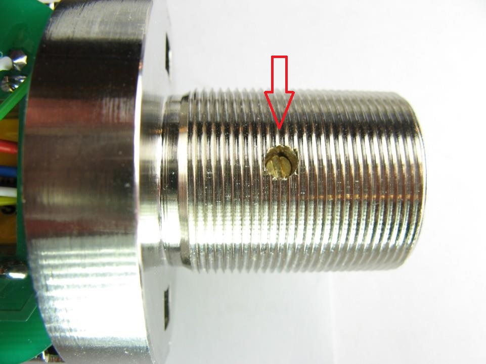
⚠️ Turret pad — high-Z connection point
The marked pad (circled in PDF p.12) is a high-impedance connection point for capsule wiring. Ensure the turret seats flush and the solder joint is clean. No flux residue on or around the turret post.
Press both Keystone teflon turrets into their PCB holes until flush with the board surface.
Solder from the underside — use minimum heat. The teflon insulation of the turret body is heat-sensitive.
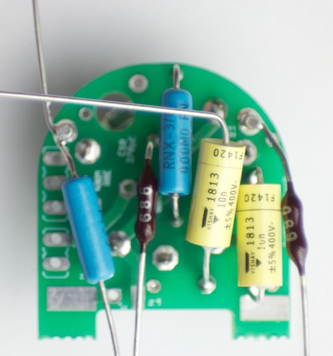
11
Install C8 & R1
C8 and R1 installedSolder side — verify joint quality
Install C8 (coupling capacitor) and R1E on the tube PCB, be sure to leave enough room (¼” or 6mm) to solder the tube socket.
Trim leads after soldering. Check both solder joints are bright and not cold.
⚠️ R1E is 400 MΩ — high-impedance handling required
Wear nitrile gloves when handling R1E. Keep the lead and joint area clean of flux residue — clean with IPA after soldering.
12
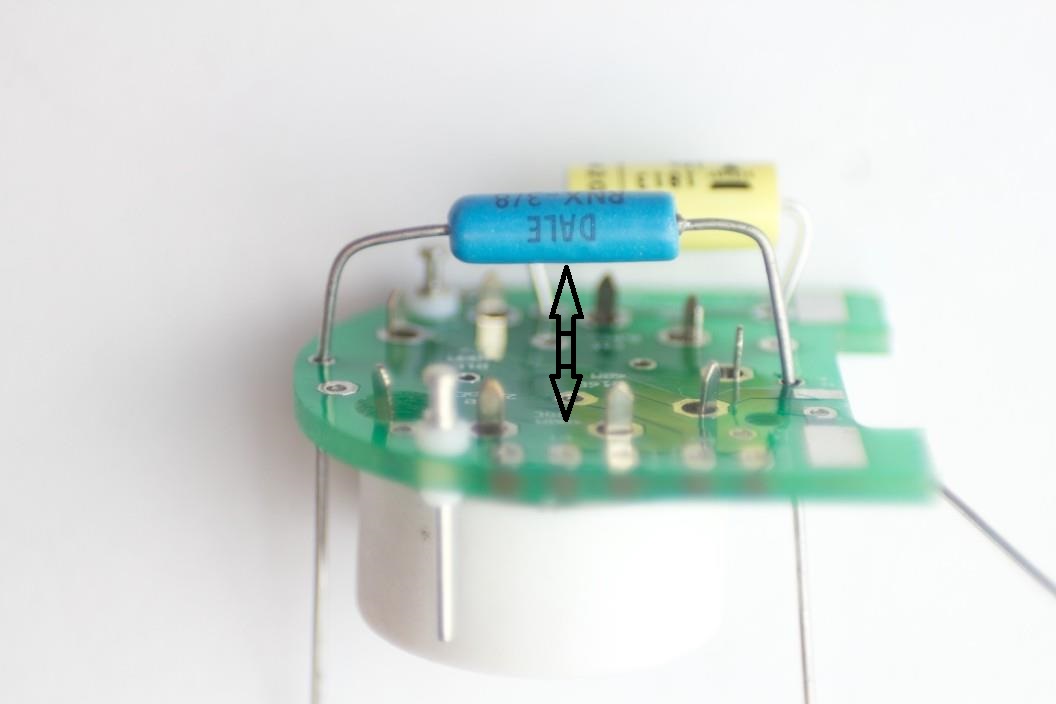
Prepare & Solder R2
Pre-form R2 leads to shapeR2 soldered to turret — see Step 20 for final routing
Pre-form R2E leads as shown before inserting into the PCB.
Solder R2E to the turret pad. This component will be further bent and routed in Steps 20–21.
⚠️ R2E is 68 MΩ — high-impedance handling required
Wear nitrile gloves when handling R2E. Keep the lead and joint area clean of flux residue — clean with IPA after soldering.
⚠️ C1 is a polystyrene (styroflex) capacitor — heat-sensitive
Heat damage to C1 is invisible at build time but causes intermittent failures. Clip an alligator-clip heat sink to the lead between the body and the PCB before soldering. Maximum iron contact: 2 seconds.
Install C1 (polystyrene) with alligator-clip heat sink on lead. Minimum iron time.
Install R16E flush to the PCB. C1 will be bent to final shape in Step 15.
⚠️ R16E is 68 MΩ — high-impedance handling required
Wear nitrile gloves when handling R16E. Keep the lead and joint area clean of flux residue — clean with IPA after soldering.
14
Prepare R8; Install Tube Socket
Pre-form R8 leadsEF86 9-pin noval socket — do not solder all pins yet
Pre-form R8E leads to shape as shown — it will be bent 90° in Steps 17–18.
Press the EF86 9-pin noval socket into the PCB. Do not solder all pins at this stage — gate pin is soldered in Step 16, remaining pins after final positioning in Step 19.
⚠️ R8E is 400 MΩ — high-impedance handling required
Wear nitrile gloves when handling R8E. Keep the lead and joint area clean of flux residue — clean with IPA after soldering.
15
Bend C1 to Shape
First bend — C1 tiltedSecond bend — C1 to final position
Bend C1 in two stages as shown. The body lays flat after both bends.
Bend at the lead, not at the capacitor body. Polystyrene bodies crack under stress.
16
Solder Tube Socket Gate Pin
Solder gate pin only — verify socket is square to PCB first
Before soldering, verify the socket sits square to the PCB from both the top and side.
Solder the gate pin only. The remaining socket pins are soldered in Step 19 after the tube PCB is seated into the body.
17
Bend R8 to 90°
First 90° bend of R8R8 in final 90° standing position
Bend R8 to stand 90° off the PCB surface as shown. Follow both images for the correct bend geometry.
R8 lead must clear adjacent components after bending.
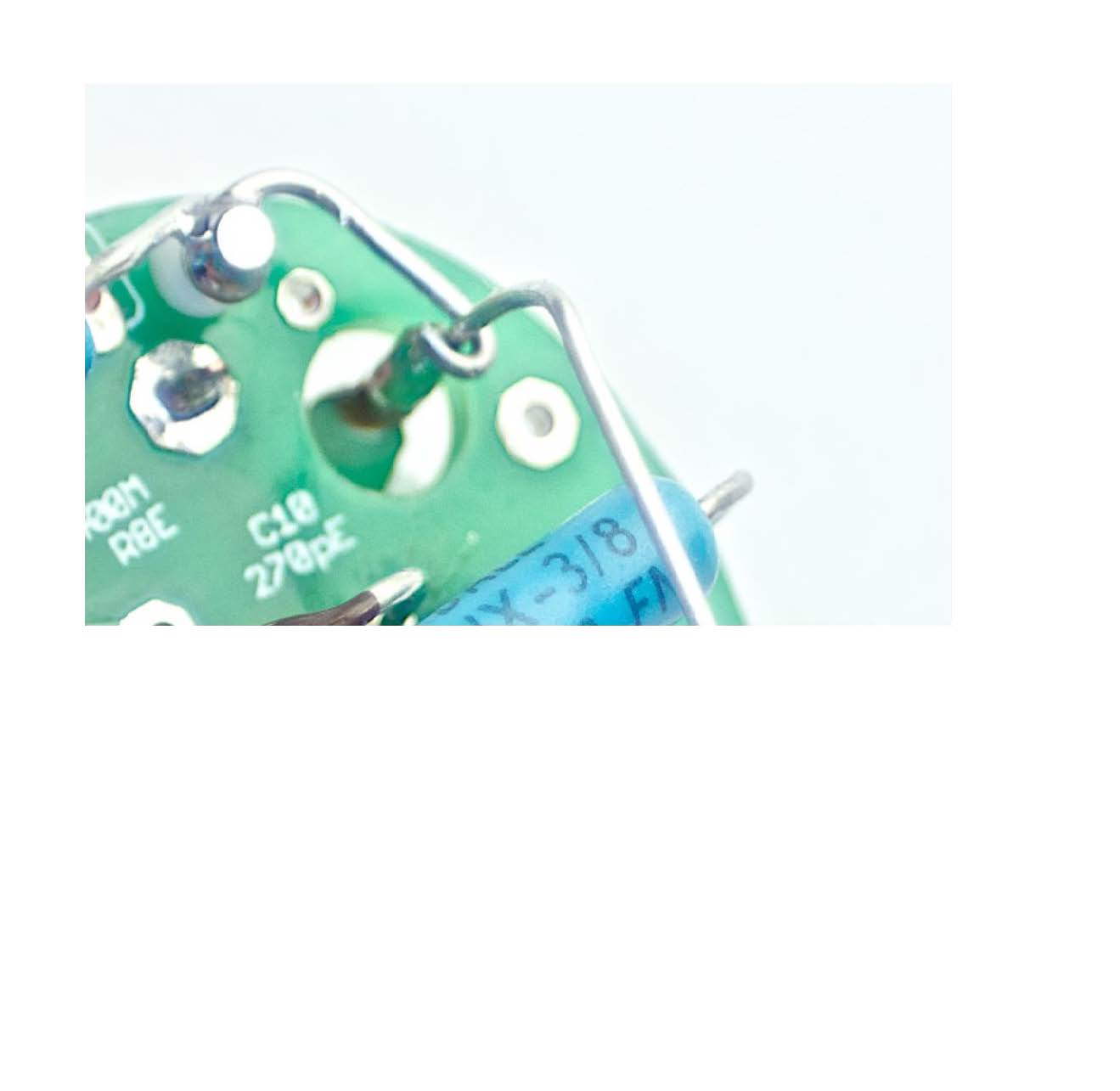
⚠️ C10 is polystyrene (styroflex) — alligator-clip heat sink required
C10 is a 270 pF polystyrene capacitor. It is heat-sensitive: clip a heat sink to the lead between the body and PCB before soldering. Maximum iron contact: 2 seconds.
Install C10 with heat sink on lead. Verify orientation per silkscreen.
After soldering, clean with IPA. Do not apply IPA directly to the installed cap body — use a brush on the pad area only.
IS jumper — install by default
The IS jumper closes S2, engaging full bass extension. Without it, the mic operates in broadcast mode with a ~200 Hz low-cut rolloff — a valid intentional choice, but not the standard setting. Install the IS jumper unless you specifically want the broadcast character.
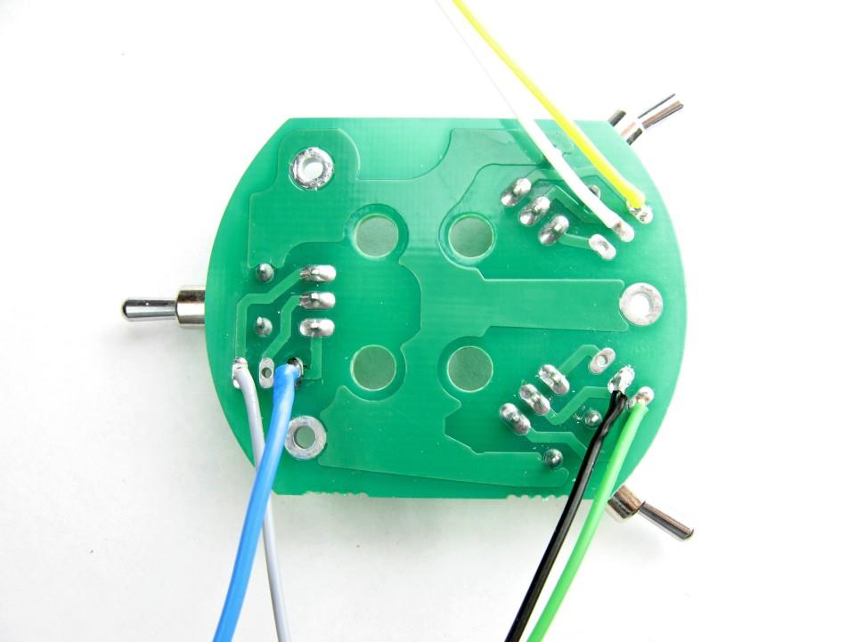
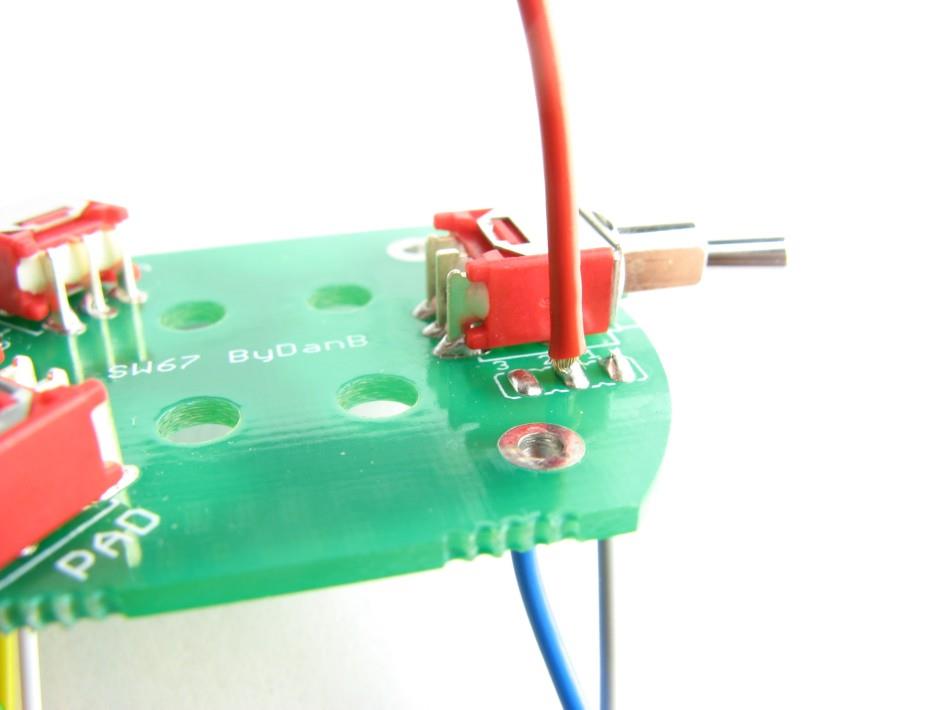
Install S1 (3-position pattern switch: Omni / Cardioid / Figure-8) and S2 (2-position switch) per the PCB silkscreen.
Verify correct orientation of S1 — the switch actuator position must match the intended panel orientation.
Install the IS jumper to bridge S2. The LC jumper is optional (low-cut).
26
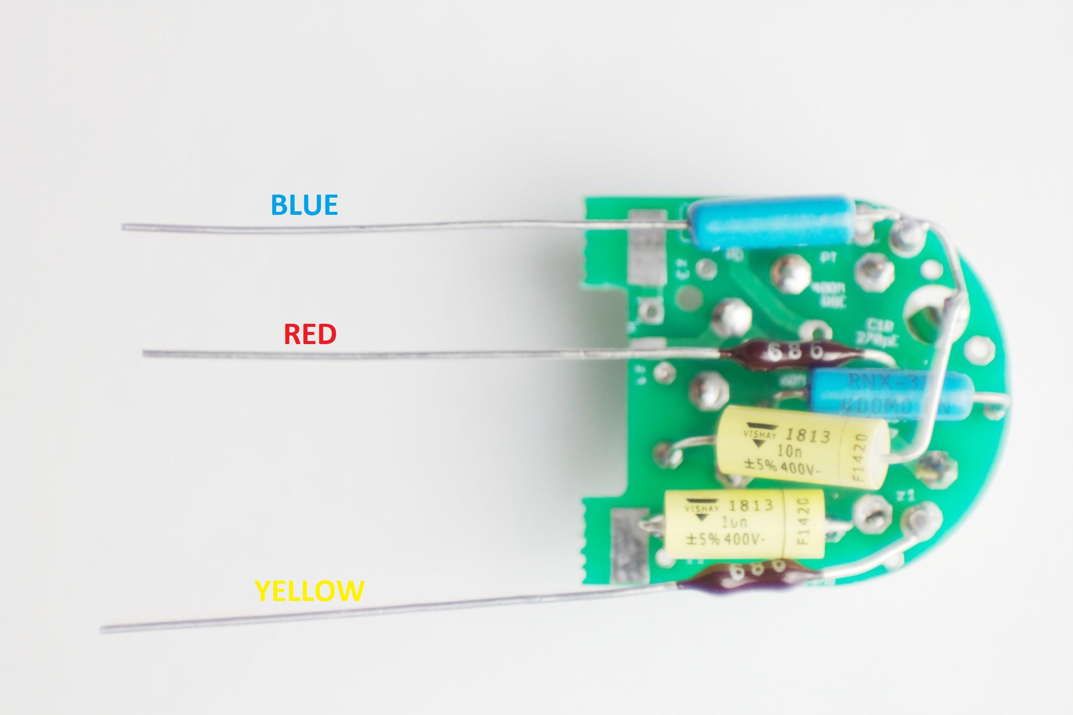
Solder Capsule Diaphragm Wires
6-color wire set soldered to capsule pad positionsRear diaphragm (RD) wire soldered
⚠️ Capsule diaphragm wires — minimum heat, pre-tin all wires
Pre-tin all capsule wires before bringing them near the capsule. Keep the diaphragm cover in place until the last possible moment. Never touch the diaphragm membrane — one fingerprint destroys sensitivity permanently.
Solder the 6-color wire set to the capsule pad positions. Use minimum iron time.
Solder the rear diaphragm (RD) wire. The front diaphragm (FD) wire is soldered at the same session.
Keep wires as short as practical — enough slack for routing but no excess.
27
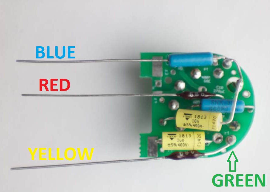
Capsule Wiring Reference
Capsule wiring reference — study before proceeding to Step 28
Study this reference before completing capsule wiring. It shows the complete wiring topology for the K67-style capsule on the D-U67.
The K67 capsule has 3 connections: BP (backplate), FD (front diaphragm), RD (rear diaphragm).
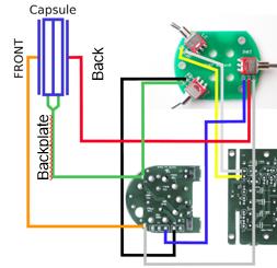
28
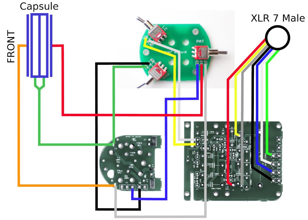
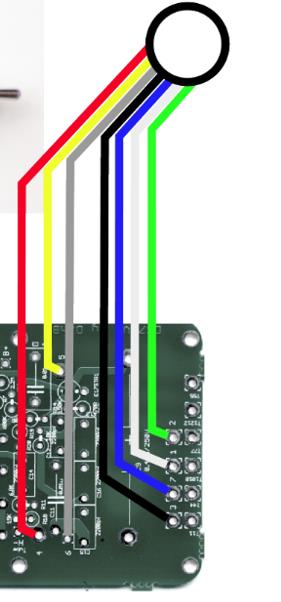
Connection Diagram Overview
Full connection diagram — Capsule → Main PCB → Tube PCB → XLR 7-pin male
This diagram shows the complete signal and wiring path from the K67 capsule through both PCBs to the 7-pin XLR output connector.
Keep this reference image visible during Steps 29–37.
29
Mount Rear Capsule
Rear capsule positioned in mountMain PCB alongside — reference for wire routing
Mount the rear capsule element in the correct orientation. Handle by the rim only — never touch the diaphragm.
Keep the protective cover over the diaphragm until final closure.
30
Feed Backplate Wire
Feed BP (backplate) wire through routing path to PCB
Feed the backplate (BP) wire through the routing path shown. The BP wire carries the capsule polarization voltage — do not short to the body.
Leave enough slack for final connection to the PCB turret but route cleanly without loops.
31
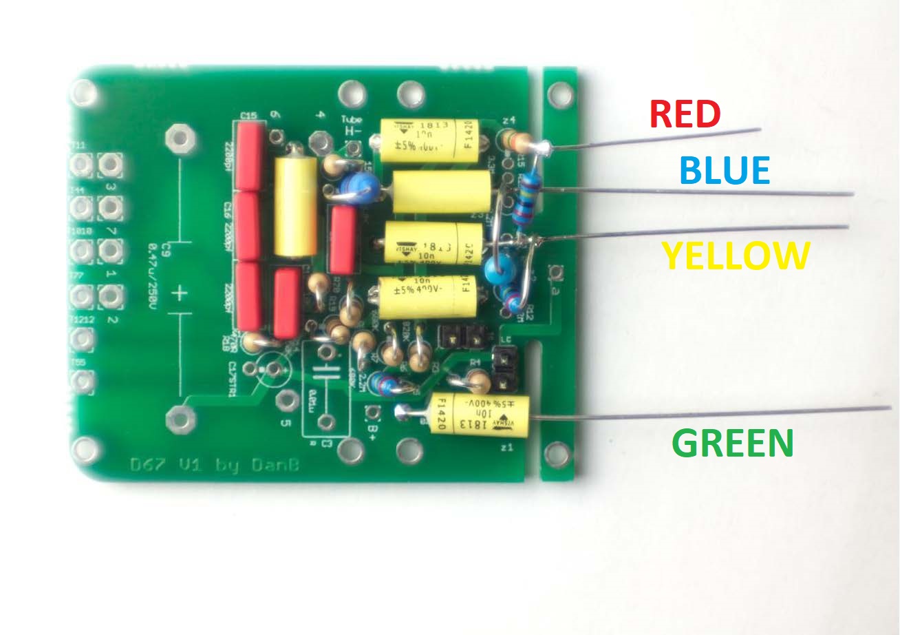
Solder Backplate & Pad Wires
Solder BP wire at red-marked padFeed pad wire through guide to positionPad wire 2 at red-marked pad
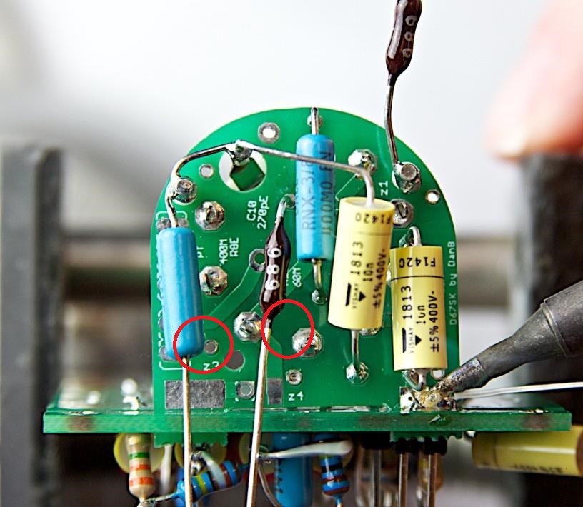
⚠️ Red zones — critical solder points (PDF p.34)
Two pads are marked with red ellipses in the PDF guide on this page. These are the critical backplate and pad wire connection points. Verify each wire lands on the correct pad before soldering.
Solder the BP wire to the pad marked in the first image (red ellipse in PDF).
Feed pad wire through its routing guide, then solder to the second red-marked pad.
Verify all joints are clean. The BP node is high-impedance — no flux residue.
32
Low-Cut & Omni Wires
LC (low-cut) wire routed to switchTrim omni wire — red zone marks connection point
⚠️ Red zone — omni wire connection point (PDF p.35)
The PDF marks the omni wire connection point with a red ellipse. Trim the wire to land precisely at this point. An incorrect length leads to strain or a missed connection.
Route the LC wire to the low-cut switch position as shown.
Trim the omni wire to the length shown — it connects at the red-marked point.
33
Figure-8 Wire
Blue figure-8 wire — red zone marks connection point
⚠️ Red zone — figure-8 connection point (PDF p.36)
The PDF marks the figure-8 wire connection point with a red ellipse. Verify the blue wire routes to and terminates at this specific point.
Route the blue figure-8 wire to the point marked with the red ellipse in the PDF. Solder.
Keep this wire isolated from the omni and cardioid wires — they carry pattern-switch voltages.
34
Complete Capsule Wiring
Cut remaining wires to ~2–3 inchesCover diaphragm with protective sleeve before final assemblyCompleted capsule wiring — verify all connections before closing
Trim remaining capsule wires to approximately 2–3 inches as shown.
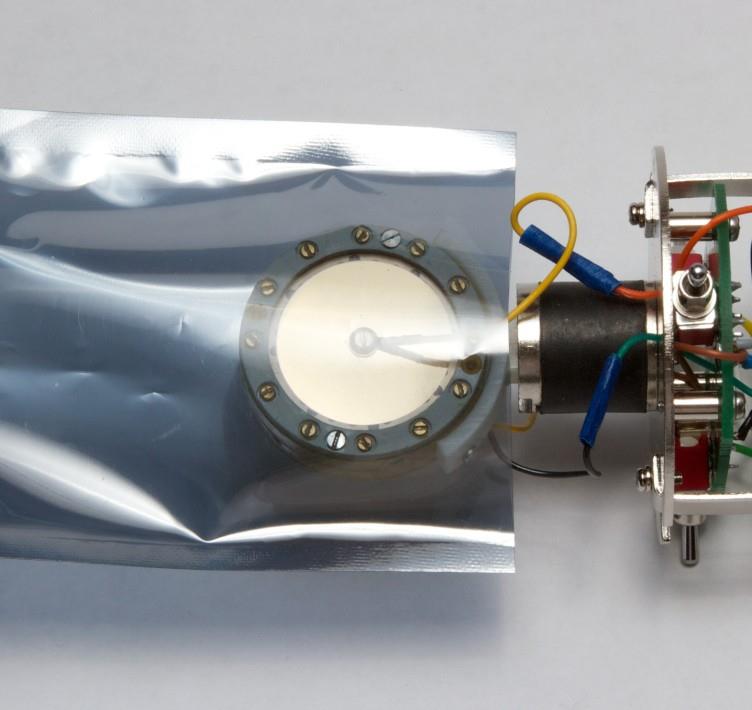
Place the protective sleeve/cover over the diaphragm before closing the assembly. It stays in place until the headbasket is fully closed.
Verify every capsule connection (BP, FD, RD) against the connection diagram from Step 28.
35
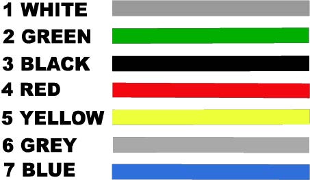
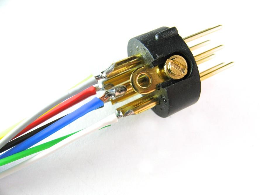
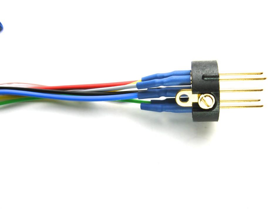
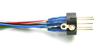
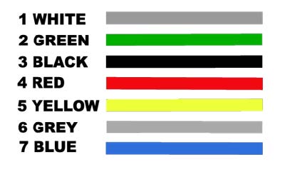
XLR 7-Pin Connector Wiring
Remove XLR insert from housing before solderingColor code table — reference for pinout
Wires soldered to XLR pinsHeat-shrink over each joint before reassembling connector
Pin
Colour
Signal
1
White
— (shield/chassis ground)
2
Green
Audio +
3
Black
Audio −
4
Red
B+ high voltage supply
5
Yellow
Polarization / pattern
6
Grey
H− heater negative (−6.3 V)
7
Blue
GND / reference
⚠️ Pin 4 (Red) carries ~210 V DC — insulate with heat-shrink
The B+ supply wire is high voltage. Apply heat-shrink tubing over the solder joint and verify no exposed conductor can contact the mic body or adjacent pins.
Remove the XLR insert from its housing before soldering — work on the free insert.
Solder each wire per the colour table above. Apply heat-shrink over every joint before reassembling.
Verify Pin 4 (Red, B+) is fully insulated from all other pins after reassembly.
36
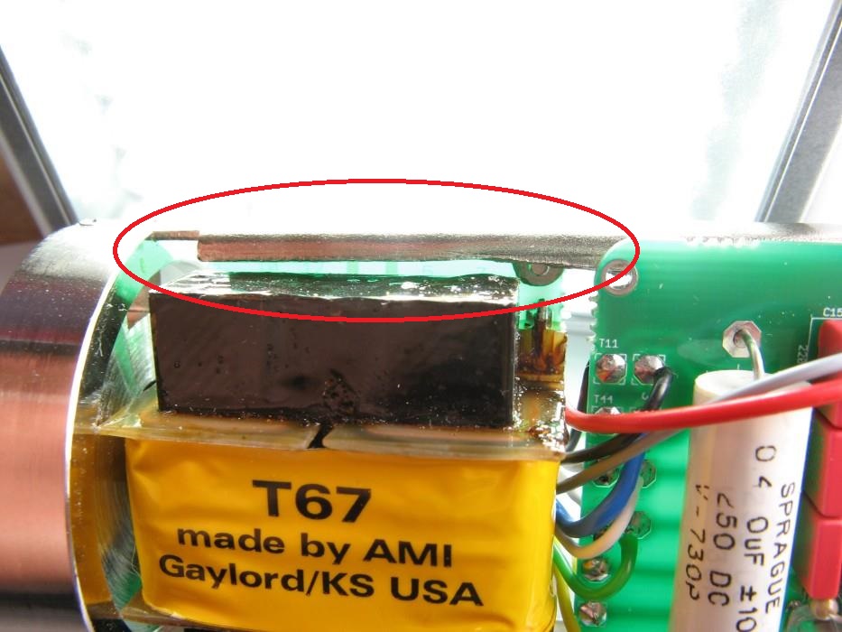
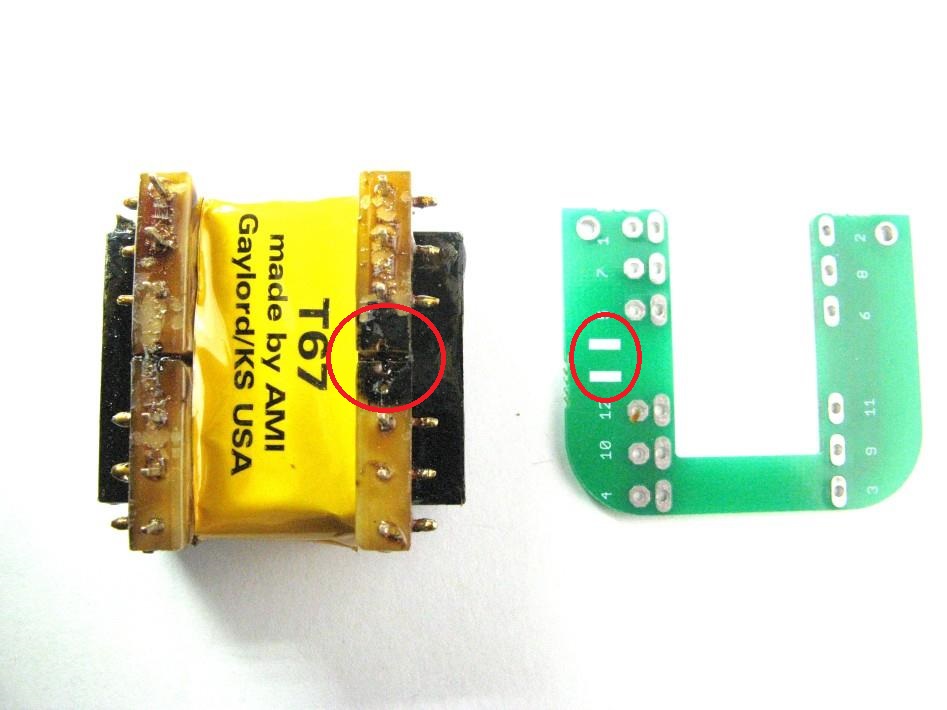
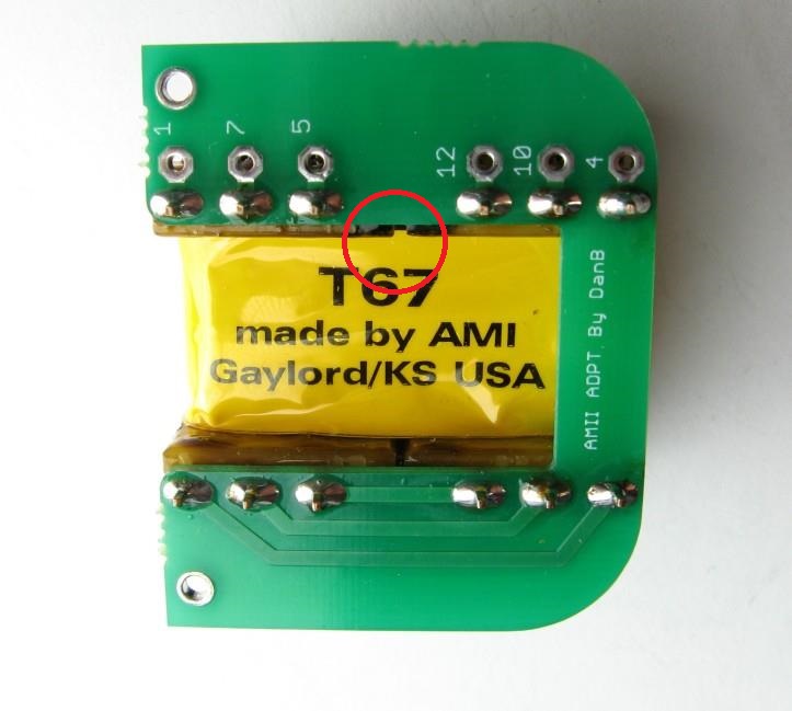
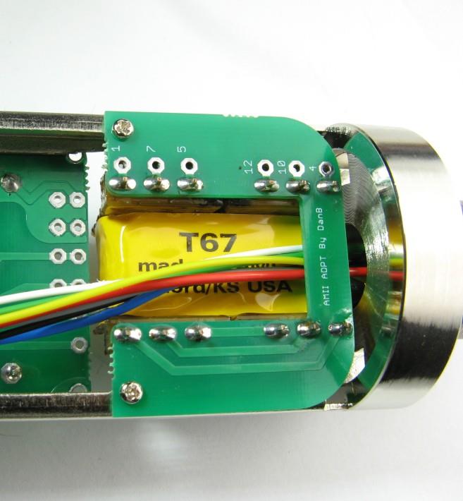
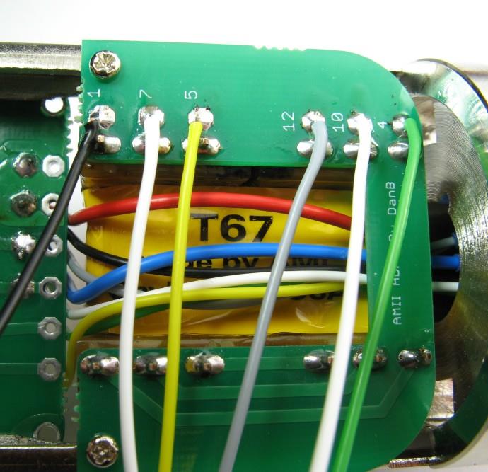
Transformer Installation (Moby BV.12)
Trim transformer PCB to required clearanceCutting tool for PCB trimVerify clearance at red-marked area before mounting
Two critical installation points (red ellipses in PDF p.41)Verify wire routing at red-marked point (PDF p.42)Transformer PCB secured with screws
⚠️ Moby BV.12 output polarity inversion
When the Moby BV.12 is wired per its own spec sheet, the output polarity is inverted relative to D-U67 PCB convention. The fix is simple: swap XLR pins 2 and 3 (audio + and audio −). Verify with a polarity tester after final assembly.
Trim the transformer PCB to the clearance shown. Verify the red-marked clearance zone (PDF p.40) before mounting.
Install the transformer PCB. The PDF marks two critical points on p.41 (two red ellipses) and one on p.42 — verify wire routing and component seating at each.
Secure with screws. Do not overtighten — the PCB material is fragile.
▶ About the Moby BV.12 transformer
The Moby BV.12 is the recommended replacement for the original Haufe BV.12. The IOaudio BV-12 has been discontinued and has a confirmed winding defect in some batches (shorted tertiary turns) that requires removing C17. The AMI T67 is also compatible but requires a different C17 value (~300+ pF). See the FAQ for C17 calibration procedure.
37
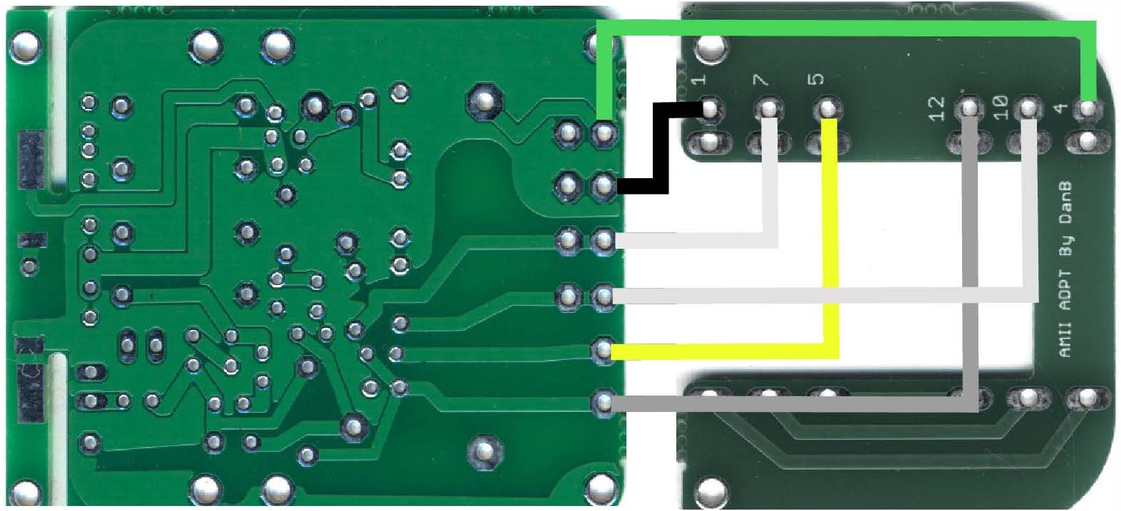
Final Wiring to PCBs
XLR wires routed to PCB positionsVerify wire colors at PCB padsXLR connection diagram — final reference
Solder wires to main PCB padsComplete wiring between main PCB and transformer PCB
Route each XLR wire to its corresponding PCB pad per the connection diagram. Verify wire colors against the colour table from Step 35.
Solder wires to the main PCB first, then complete connections to the transformer PCB.
Dress all wires neatly. No wire should be under mechanical stress or cross the mic body seam.
Before closing: measure DC resistance from each XLR pin to PCB ground to catch any shorts. Then connect to PSU and verify voltages per the PSU section below.
Build complete — verify voltages before installing the tube
Power up the PSU with the mic connected but tube not yet installed. Verify B+ ~210 V and H− ~−6.3 V at the PCB. Only install the EF86 tube after voltages are confirmed correct.
38
First Power-On & Calibration
⚠️ Tube not yet installed for voltage check
Power up the PSU with the mic connected but the EF86 tube not yet seated. Confirm B+ ~210 V and H− ~−6.3 V at the PCB pads. Only proceed with the tube once voltages are confirmed.
Power off. Seat the EF86 tube fully into the socket — verify all pins engaged, no bent pins.
Power on. B+ will start high (240–320 V unloaded) and drop as the tube heats up — this is normal. Do not adjust trimmers yet.
Let the tube warm up for 15–20 minutes before taking any measurements or adjusting anything.
After warm-up, measure B+ at the designated test pad (DMM − to 0V pad). Target: ~210 VDC (205–214 V acceptable).
Measure H− at the heater test pad. Target: ~−6.3 VDC (±5% acceptable). Being slightly under is preferred.
If adjustment is needed: trim Rtrim H− first to reach −6.3 V, then trim Rtrim Plate to reach 210 V B+.
Monitor continuously during warm-up — sniff for any unusual smell. If anything smells, power off immediately and inspect before continuing.
If the 56 kΩ trim range is insufficient
If the B+ trimmer can't reach 210 V at its full range, replace the 56 kΩ fixed resistor with 47 kΩ to shift the trim window down.
Power off. Install the mic body — the body provides the required ground path for the pattern switch PCB.
Power on. Connect to a mic preamp and monitor through headphones.
Test the LC (low-cut), Pad, and pattern switches one at a time — you should hear clear changes for each.
Speak into the mic — congratulations on completing your D-U67 tube condenser build.
Stuck?
Common problems, solved
Answers synthesized from the D-U67 community thread and build reports. Search before posting.
🔍
No matching questions — try a different search term or clear the filter.
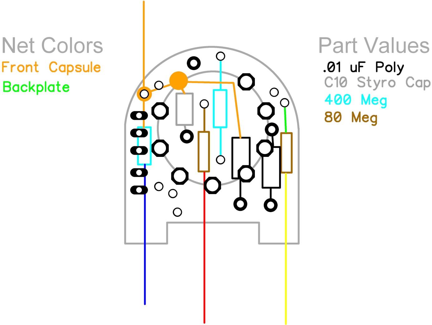
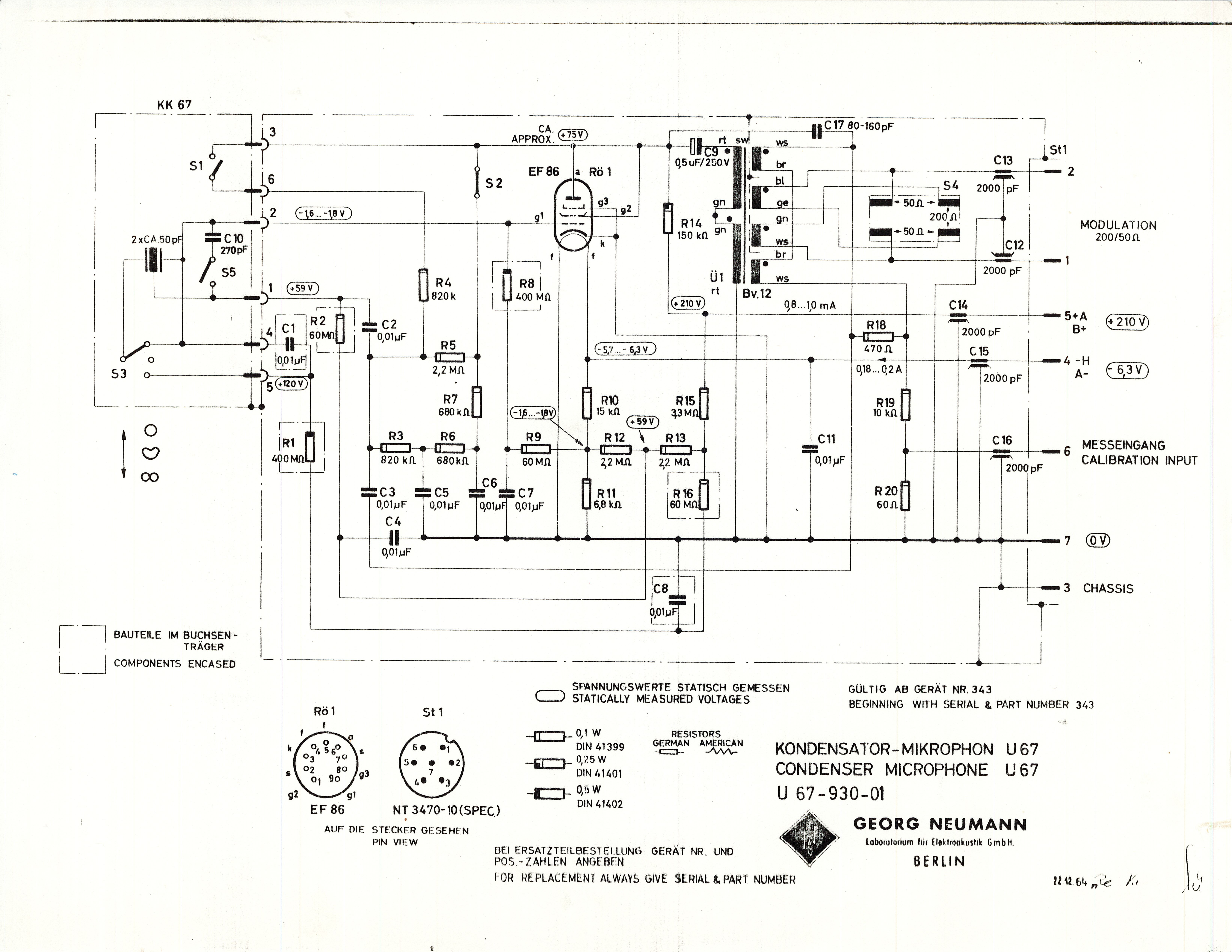
Circuit Reference
Click to enlarge · Neumann U67-930-01 — EF86 pentode circuit
Key nodes: B+ = ~210 V (plate supply from PSU); H− = −6.3 V (EF86 heater negative supply); S1 = pattern switch (Omni / Cardioid / Figure-8); S2 = internal switch, closed by IS jumper; BV.12 = output transformer (Moby BV.12 recommended); C17 = de-emphasis capacitor, transformer-dependent — calibrate by CAL sweep.
Component List
D-U67 Microphone BOM
Components for the microphone PCBs (main + tube). PSU designators are on a separate board — see PSU BOM below.
#
Ref
Qty
Value
Description
Part / Notes
Type
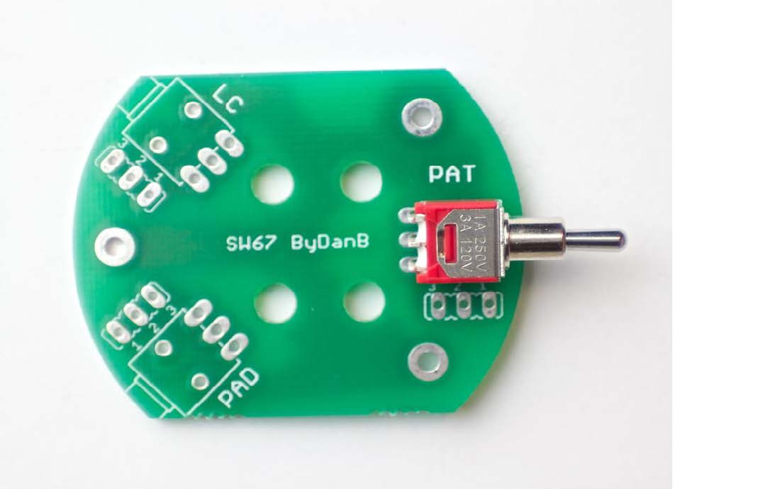
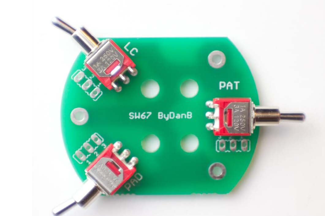
PSU Assembly
7 steps
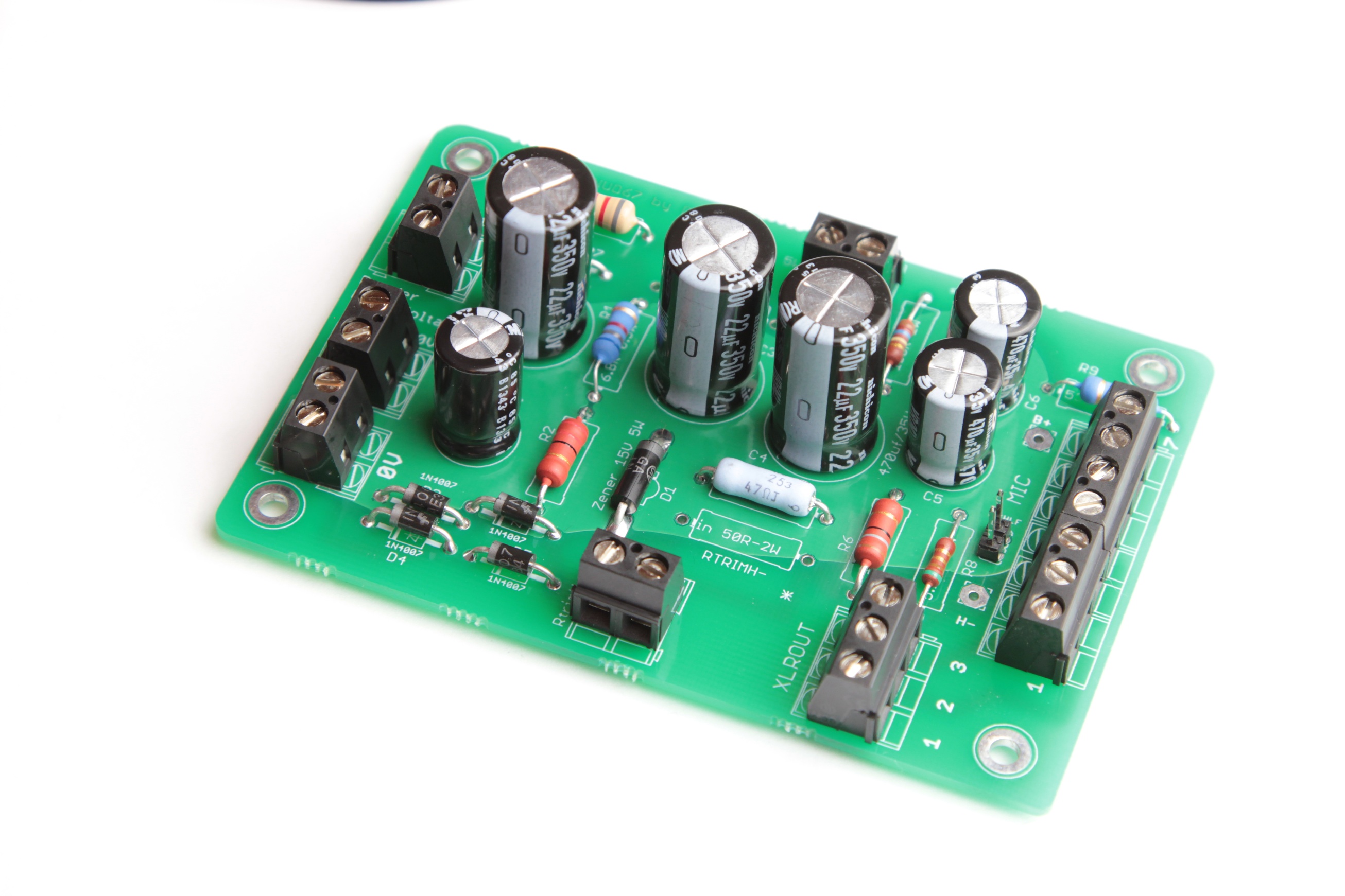
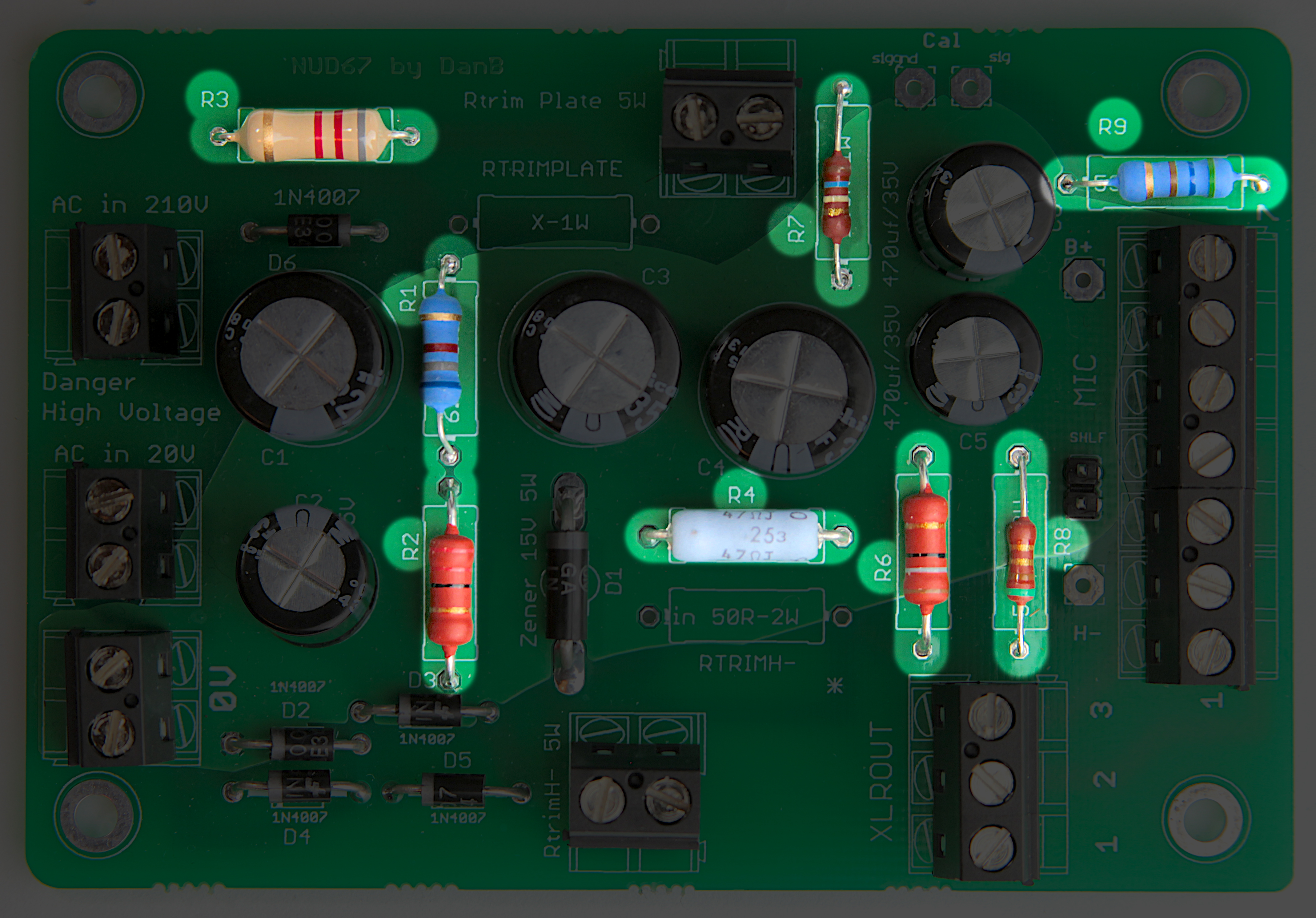
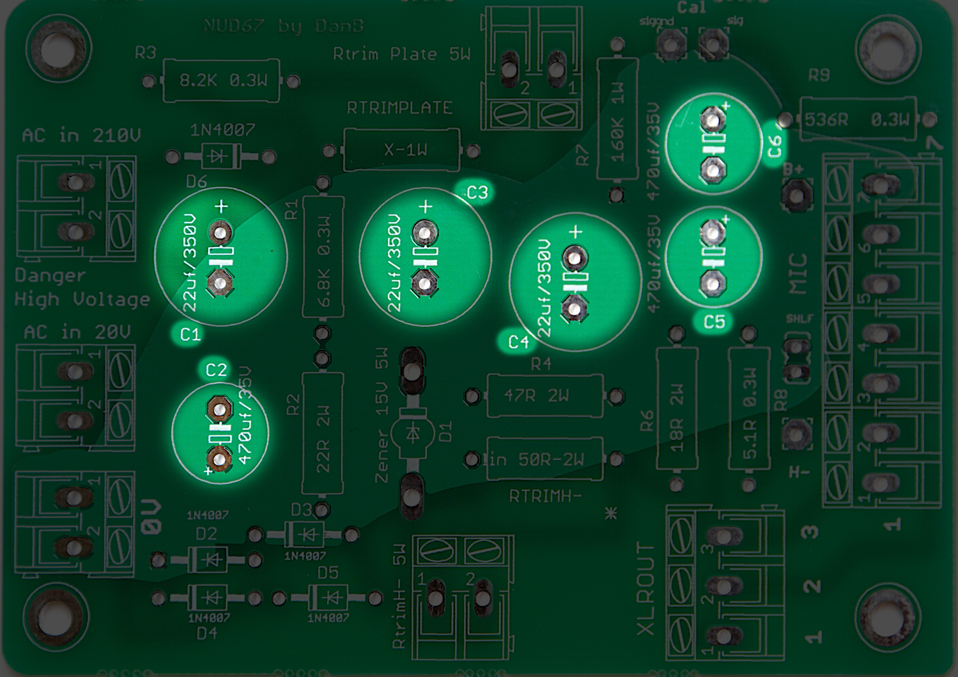
P1
PSU PCB Overview
PSU PCB — reference for final assembly
Study this reference image before populating the PSU PCB. It shows the completed board.
Populate components in order: resistors first, then diodes, electrolytic capacitors, headers. The SHLF jumper is last.
The PSU handles mains-derived voltages up to ~210 V DC. Build and verify in an isolated environment. Do not connect to the mic until all voltages are confirmed on the bench.
P2
Tools
Temperature-controlled iron — fine tip0.6–0.8 mm rosin-core solder
Flush-cut lead cuttersAcid brush + 91 % IPA
Temperature-controlled iron, 25–40 W, fine tip, ~350 °C.
Flush-cut lead cutters — cut leads close to the PCB after soldering.
91 % IPA + acid brush for cleaning flux residue between steps.
P3
Install Resistors
All resistors placed — bend leads under PCB to hold in placeLong leads before trimLeads trimmed flush after soldering
Start with the resistors — they are the lowest-profile components and easiest to populate first.
Stuff all resistors, then bend the leads inward on the bottom so components stay in place without taping. Verify no bent lead overlaps a trace or pad that could cause a bridge.
Clip all leads flush after soldering. Inspect each joint: bright, smooth, no cold solder or bridges.
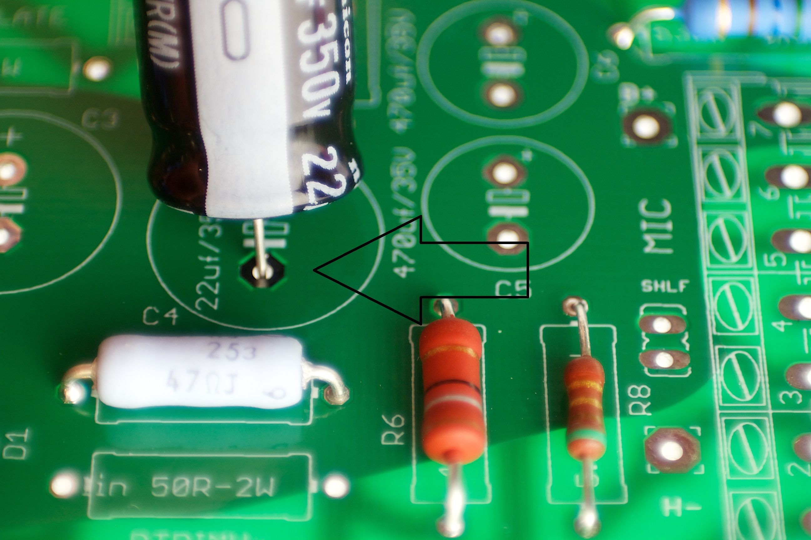
R2 (22 Ω / 5 W): must stand off the PCB surface ~5 mm to allow airflow. Do not install flush.
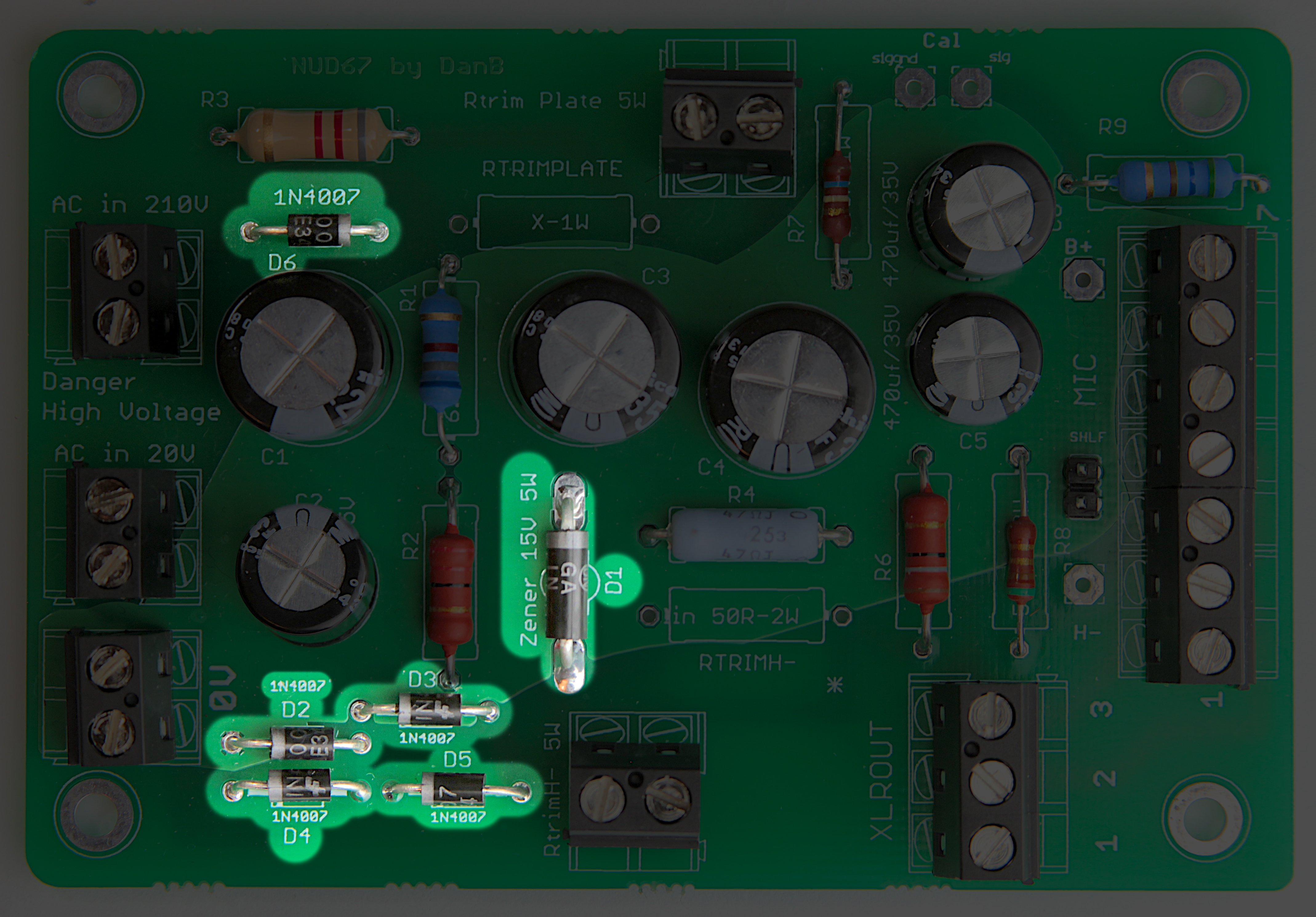
P4
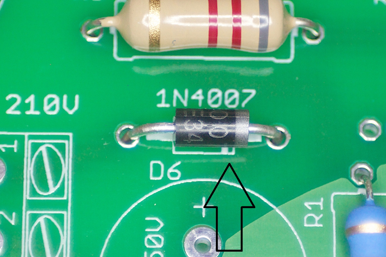
Install Diodes
D2–D6 placed — verify polarity before solderingCathode band aligned with PCB line
⚠️ Diode polarity — cathode band must match PCB line
The PDF guide marks the cathode alignment point with an arrow on this image. The grey or white band on the diode body is the cathode — align it with the line printed on the PCB silkscreen. A reversed diode will prevent the rectifier from operating and may damage other components.
Install D2–D6 (1N4007). Verify polarity on every diode before soldering: cathode band on diode body → line on PCB silkscreen.
Bend leads to hold components in place, then solder all, then clip leads flush.
P5
Install Electrolytic Capacitors
Electrolytics placed — verify polarity before solderingWhite stripe = negative — align with white band on PCB
⚠️ Capacitor polarity — white stripe is negative (−)
The PDF guide marks the polarity band with an arrow on this image. The white stripe on the capacitor body is the negative lead. Match the white stripe on the cap to the white band printed on the PCB. A reversed electrolytic capacitor can fail violently under voltage.
Install C1, C3, C4 (22 µF / 350 V) and C2, C5, C6 (470 µF / 35 V). Verify polarity on every capacitor.
The longer lead is positive (+); the white/light stripe on the body is negative (−). Both indicators must agree with the PCB marking before soldering.
The 350 V–rated capacitors (C1, C3, C4) are taller — verify they clear the enclosure lid if applicable.
P6
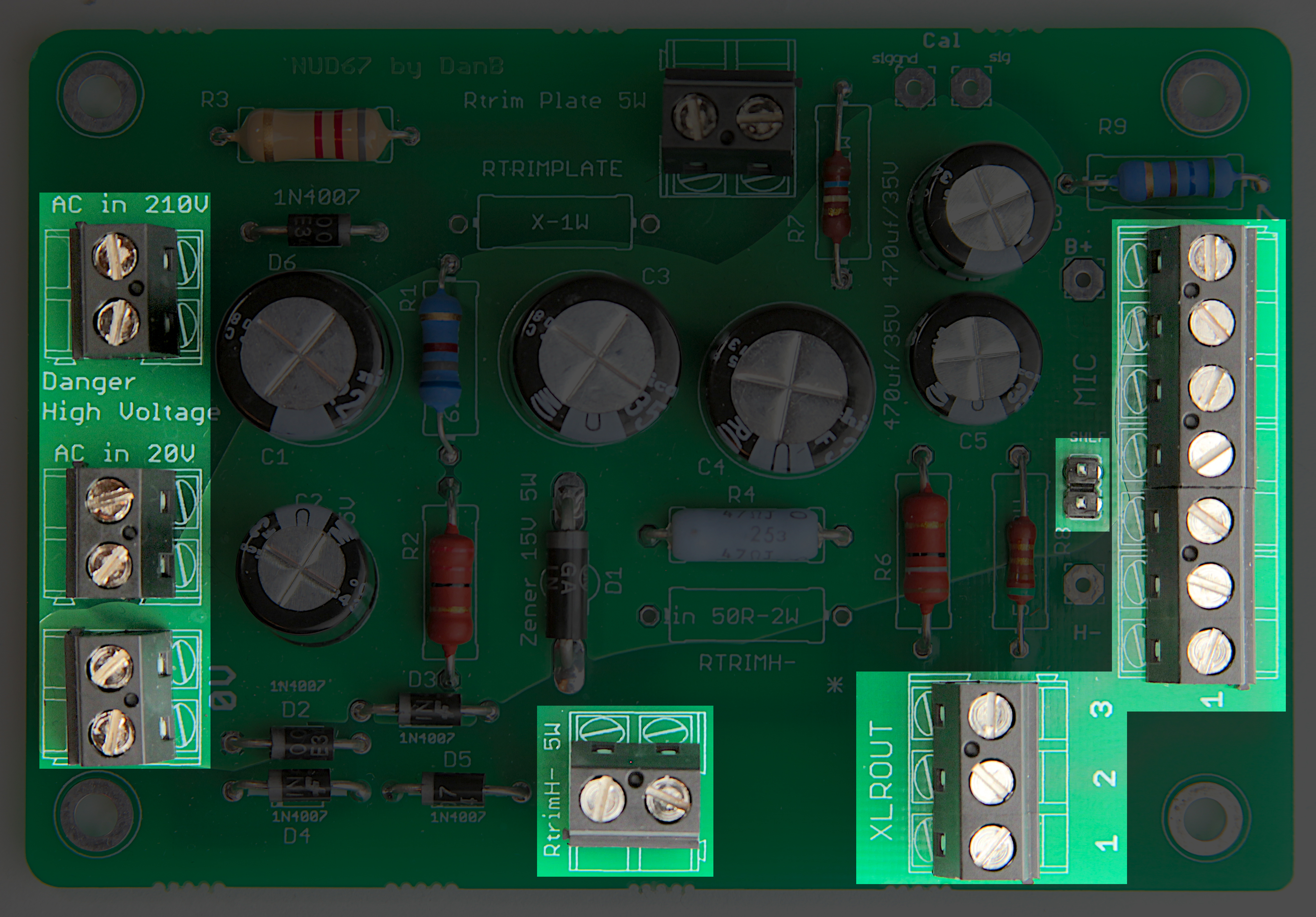
Install Headers & Wire Terminals
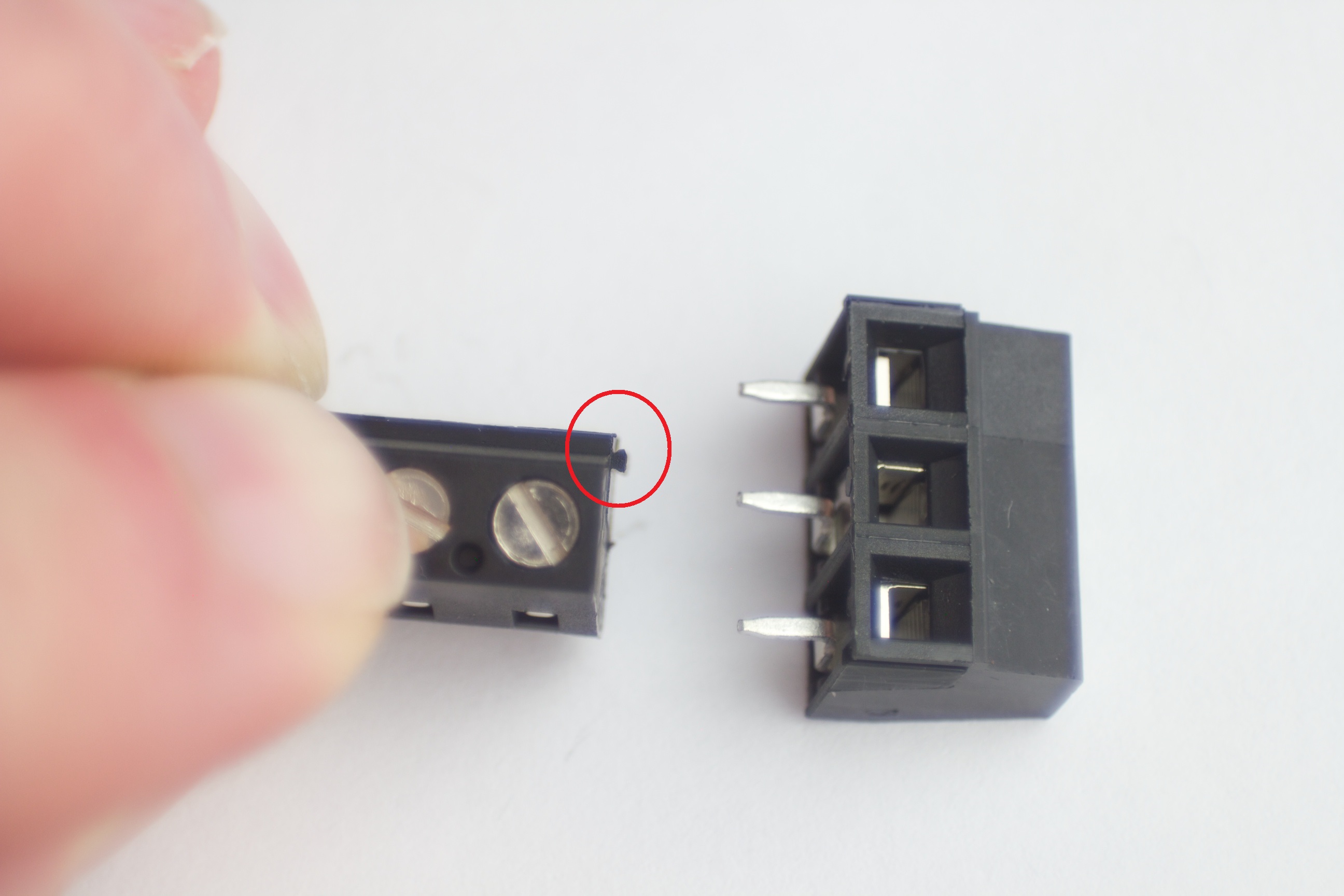
Headers and terminal blocks placed on PCBRed zone — dovetail interlock between 4-pin and 3-pin terminals
⚠️ Red zone — connector interlock (PDF p.6)
The PDF marks the dovetail interlock between the 4-pin and 3-pin terminal blocks. Interlock the two connectors before installing on the PCB — the dovetail feature ensures they are correctly joined. Once interlocked, treat them as a single connector for soldering.
Interlock the 4-pin terminal block to the 3-pin terminal block using the dovetail locking feature shown.
Place the interlocked connector on the PCB. Solder one pin of each connector first — inspect and adjust to ensure both sit square and flush before completing all pins.
Install the SHLF jumper (solder bridge between both SHLF pads — this is mandatory for star ground).
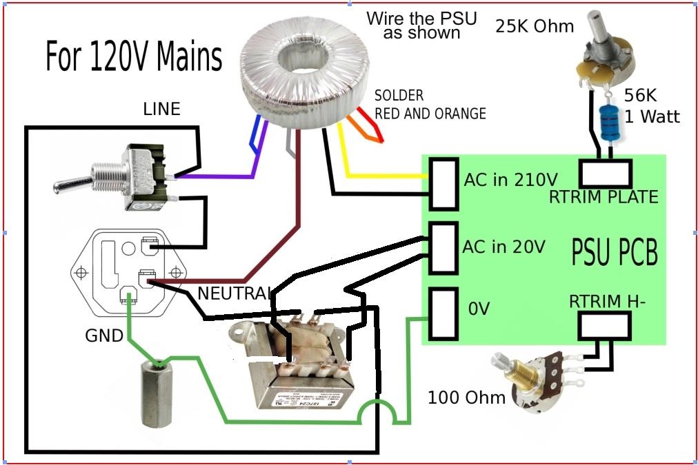
Use this wiring schematic to connect the two external power transformers (VPT230-110 at X3, Hammond 186B20 at X2) to the PSU PCB.
Connect the 7-pin XLR cable output per the diagram. Verify wire colors against the table in Step 35 of the mic build guide.
Before connecting the mic: power up the PSU on the bench with a multimeter, measure B+ (~210 V DC) and H− (~−6.3 V DC). Adjust trimmers. Connect the mic only after both voltages are confirmed.
First power-up sequence
1. Verify PSU voltages on bench (no mic connected). 2. Adjust RTRIMH to −6.3 V. 3. Adjust RTRIMPLATE for target B+. 4. Connect mic (tube not installed). 5. Verify voltages at mic-side XLR. 6. Install EF86 tube. 7. Allow 5-minute warm-up before audio test.
D-U67 PSU BOM
Components for the PSU PCB. Power transformers (VPT230-110 HV + Hammond 186B20 heater) are external to the PCB and not listed here.
#
Ref
Qty
Value
Description
Part / Notes
Type
Power Supply
External PSU — builder-assembled
D-U67 PSU — outputs
Builder assembled
The D-U67 uses an external PSU connected via a 7-pin XLR cable. The PSU provides two regulated supplies for the EF86 pentode:
B+ supply: ~210 V DC — plate supply for EF86. Regulated via D1 Zener (15 V / 5 W).
H− supply: ~−6.3 V DC — heater negative supply (EF86 heater is referenced to negative rail). Trim with RTRIMH to exactly −6.3 V.
Verify both supplies on the bench before connecting the mic. Adjust RTRIMH for −6.3 V heater voltage and RTRIMPLATE for target B+. Allow 5 minutes warm-up before measuring.
Power transformers
External to PCB
Two transformers are required, external to the PSU PCB:
VPT230-110 — HV transformer (mains to ~210 V AC secondary). Provides B+ supply input at X3 connector.
Hammond 186B20 — Heater transformer (20 V / 6 VA). North America standard. Provides H− supply input at X2 connector.
Both transformers must be mounted in a chassis with proper mains isolation and fusing. The PSU handles mains voltages — build to local electrical safety standards.
SHLF jumper & star ground
Mandatory
The SHLF jumper on the PSU PCB must be installed. It connects the mic cable shield at the PSU end (star ground topology). Without the SHLF jumper, the cable shield is ungrounded and the system will be susceptible to interference.
SHLF = Shield at PSU end — one solder bridge or 0 Ω jumper between the two SHLF pads.
The shield wire in the 7-pin XLR cable connects to Pin 1 (White) and is grounded at the PSU only, not at the mic body end.
Ready to build?
The complete D-U67 kit — body, main PCB, tube PCB, component set, and K67 capsule — available at microphonediy.com.