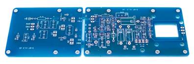
Unpack and verify contents against the BOM — 40 components total (canonical 2026 rev 1R0a).
Sort resistors and capacitors by value before touching the iron.
Confirm tools: temperature-controlled iron (650–700 °F), 0.6–0.8 mm solder, multimeter, isopropyl alcohol ≥ 91 %, nitrile gloves.
Read this entire guide and the Errata section before placing a single component.
⚠️ Counterfeit 2N3819
Widespread on eBay and unauthorized marketplaces. Fakes test as NPN BJTs (base / collector / emitter), not JFETs. Order only from Mouser, Newark, Small Bear, or NTE Parts Direct — and test every unit with a transistor tester before installation.
⚠️ Safety
Never connect or disconnect the microphone with phantom power active. Never touch the capsule diaphragm. Keep static discharge away from the JFET and 1 GΩ resistors.
▶ 💡 Measuring JFET IDSS — 9 V battery method
Short the JFET gate and source; connect to the negative terminal of a 9 V battery; DMM in mA range, black probe to drain, red probe to +9 V. That reading is IDSS in mA. Target ≤ 10 mA; sweet spot 4–8 mA.
02
Inspect PCB
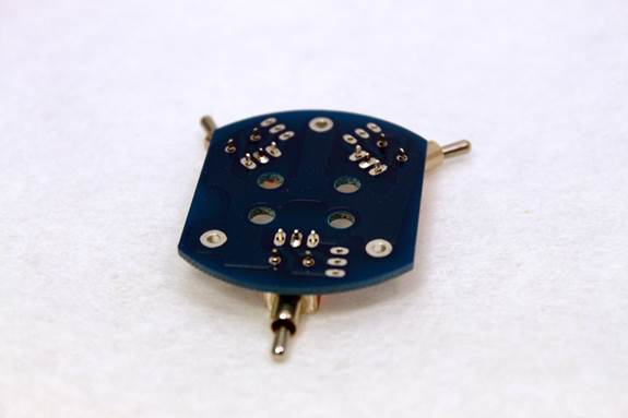
Bare D-87 PCBs before population — main board, switch board, and capsule connection board.
Lay the PCB on a clean, static-safe surface.
Identify your variant: Green (D-87L, two-board layout) or Blue (D-87M Mono-Block, single board). The build sequence differs.
Sort all components by value — resistors and caps separated and labelled before you start.
Warm up the iron; verify the tip is clean and at temperature.
⚠️ PCB version determines build sequence
The Green PCB has documented silkscreen errors (Errata E1 & E5) that the Blue PCB does not. Identify your board before placing any components.
▶ 💡 Blue PCB switch wiring (D-87M v1.3+)
Short CRD↔OMN for omni; CRD↔8 for figure-8; nothing shorted for cardioid.
03
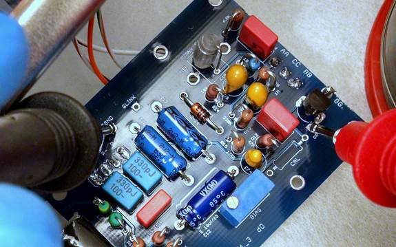
Install Resistors & Diodes
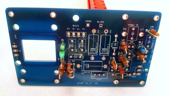
After resistor and diode installation. Zener cathode band aligned to the silkscreen indicator at lower left.
Populate all resistors first — lowest-profile parts before taller components.
Verify each value with a multimeter against the BOM before soldering.
Keep leads short; trim flush after soldering.
Install Zener diode Z-24 (1N4749A) with the cathode (banded end) aligned to the silkscreen indicator.
Select R18 and R19 as the closest-matched pair from the 5 supplied — measure each with a DMM and record.
⚠️ Errata E1 — R6 reversal (Green PCB only)
Install R6 (1 GΩ) reversed relative to the silkscreen orientation. Blue PCB does NOT require reversal. See Errata E1.
⚠️ Errata E5 — R12 / R13 silkscreen (Green PCB V1.1 / V1.2 only)
The 47 kΩ (R12) and 330 kΩ (R13) designators are visually close. Swap them and the drain is stuck near 1 V. Verify before soldering. See Errata E5.
⚠️ Reversed Zener = drain stuck at ~22 V
The single most common first-power-up failure. Triple-check polarity.
▶ 💡 R18 / R19 matching and CMRR
1 % match → ~49 dB CMRR; 0.4 % match → ~64 dB CMRR. Hand-matching from a 5-piece lot reliably achieves <0.5 % — adequate for project-studio use.
04
Install Capacitors
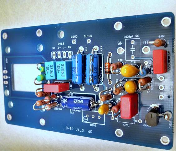
Correct polarity of electrolytic and tantalum capacitors. Yellow tantalums and blue electrolytics alongside the red WIMA film caps.
Film & ceramic (non-polar): C2, C5, C9, C14, C16, C17. Install in either orientation.
Polarized: C7, C8, C10 (tantalum); C11, C12, C13 (electrolytic). PCB "+" must match component "+". Solder one lead first, verify orientation, then the second.
Polystyrene: C1, C3, C4, C6, C15. Clean board with 91 % IPA before installing. Use thermal-mass clip or round-robin technique.
⚠️ Reversed tantalum = FET damage on first power-up
C7 and C8 are the most-often-reversed positions in documented build failures. Triple-check the "+" silkscreen marking.
⚠️ Polystyrene heat & solvent sensitivity
Heat damage is often invisible at build time but produces pops months later. IPA dissolves polystyrene; acetone destroys it. Never apply IPA or acetone near polystyrene caps once installed.
▶ 💡 Thermal-mass clip technique for polystyrene caps
Clamp an alligator clip on the component lead between the cap body and PCB (component side). Solder from the underside. The clip absorbs heat before it reaches the dielectric.
▶ 📜 Why 630 V polystyrene specifically?
Pre-2012 builds used thinner-bodied lower-voltage units that were more heat-fragile and failed years after installation. The 630 V rating makes the substrate physically robust enough to survive normal soldering.
05
High-Impedance Input Section
High-impedance section — 1 GΩ and 68 MΩ resistors. Clean solder joints are critical; any contamination directly degrades self-noise.
Components: R3, R6, R7 (1 GΩ thick-film) and R4, R5 (68 MΩ or 60 MΩ).
Use minimal flux. Inspect each joint under good light or a magnifier before moving on.
Clean thoroughly with 91 % IPA on a clean toothbrush after soldering. Keep IPA away from any polystyrene caps nearby.
⚠️ Nitrile gloves required throughout this entire step
Finger oils on the high-impedance area create irreversible leakage paths that permanently degrade self-noise. Do not touch the 1 GΩ resistor leads, their pads, or the surrounding PCB with bare hands — not even before soldering.
▶ 💡 Recovering a noisy existing build
Multiple documented cases resolved with thorough cleaning of this area alone — no component replacement. 91 % IPA on a clean toothbrush, 30–60 seconds per side; air-dry several minutes before powering up.
06
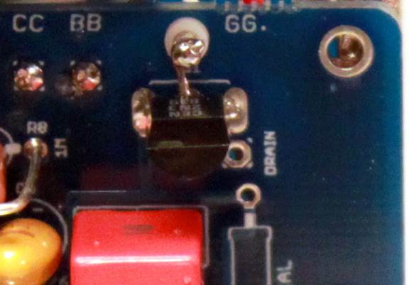
JFET Installation + Trim Pot
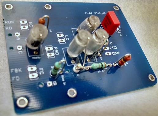
JFET installed correctly. On the Green PCB the gate (center pin) routes to a floating Teflon-isolated turret pin — never directly to the PCB pad.
Verify JFET orientation: flat side faces the silkscreen flat-side indicator; center pin (gate) → silkscreen "G".
Solder source pin first, inspect; then drain; then gate. Keep iron contact per pin under 3 seconds.
Green PCB only: solder the gate to the floating Teflon-isolated turret pin — never directly to the PCB pad.
Install the BIAS trim pot (T93YA253KT20) in the three center holes of the R11/CAL position.
⚠️ Errata E6 — NTE312 has a different pinout from 2N3819
If substituting NTE312, the gate is on an outer pin, not the center. Rotate 180° from the silkscreen orientation. Installing in the 2N3819 orientation damages the FET. See Errata E6.
⚠️ IDSS targeting: sweet spot 4–8 mA, maximum 10 mA
High-IDSS units are hard to bias. If stuck with a high-IDSS FET, see modification V17 (33 V Zener) or V26 (5.6 kΩ R17).
▶ 💡 Source / drain symmetry in the 2N3819
The 2N3819 is internally symmetric — source and drain can be reversed with only a small (~1–2 dB) SNR penalty. The gate must reach the silkscreen "G" position; that is the only invariant.
07
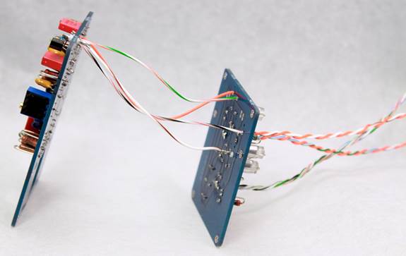
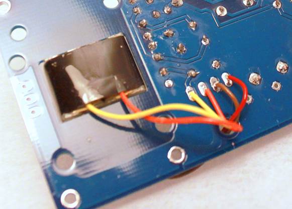
Connect Main PCB to Switch PCB
Main and switch PCBs connected by Teflon-jacketed wire.Wire routing detail — neat bundle, slight slack at each end.
Green PCB only — Blue PCB Mono-Block skips this step (all on one board).
Use 26 AWG silver-plated Teflon-jacketed wire — the community standard.
Leave slight slack; wires under tension fatigue at the solder joint over time.
⚠️ The G/GG connection is in the high-impedance area
Clean any flux residue immediately after soldering this joint.
08
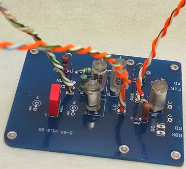
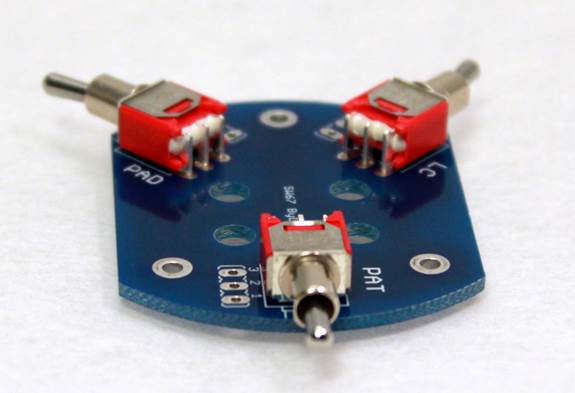
Switch PCB Installation
Switches positioned before soldering — verify each sits flat and square.Switch PCB complete — pattern selector (center, 3-position), pad and HPF on either side.
Install three toggle switches: pattern (3-position center-off), pad (−10 dB, 2-position), HPF (~50 Hz, 2-position).
Solder the middle pin of each switch first for alignment; verify it sits flat and square; then solder the remaining pins.
⚠️ Pattern-switch pop is normal
The original Neumann U-87 produces the same pop on each switch position change. Mute monitors or turn down preamp gain before switching patterns.
09
Output Transformer
Transformer mounted and wired. Always DCR-test before soldering — color codes are not standardized across manufacturers.
DCR-test before soldering, always. Higher-resistance pair = primary (capsule side, RT/SW); lower-resistance = secondary (XLR side, WS/BL). Expect ~100× ratio for a 10:1 step-down.
Keep secondary leads short. No transformer can required.
⚠️ Errata E4 — AMI / TAB-Funkenwerk T13 color code is reversed
AMI's published wiring is wrong for the U-87 application. Black wires = primary (RT/SW, ~440 Ω). Yellow wires = secondary (WS/BL, ~22 Ω). Always DCR-test before soldering. See Errata E4.
⚠️ Cinemag CM-13113 wiring is reversed from CM-2480
Use brown for primary, red for secondary. Verify by DCR.
▶ 💡 Transformer alternatives
Cinemag CM-2480 (~$30, canonical baseline); CM-13113 (~$45); AMI T13 (~$95, see E4); Sowter 1303f (UK/Europe); Moby BV.13; UTM 0587; Peluso BV11P/BV8P-S. All require DCR verification before wiring.
10
XLR Wiring
Completed XLR wiring with heat-shrink on each lead.XLR lead routing inside the body — keep runs short and tidy.
Wire the 3-pin XLR using this mapping — NOT 1:1 from the silkscreen:
Apply heat-shrink on every lead. Connect the XLR shell tab to pin 1 (chassis ground).
⚠️ Errata E3 — PCB silk labels do NOT match XLR pin numbers
Wiring 1:1 from the silkscreen produces a polarity swap or grounding fault. Use the mapping table above. See Errata E3.
▶ 💡 Continuity between XLR pins 2 and 3 — this is normal
The transformer secondary is a low-DCR coil; pins 2 and 3 connect through it. Use the Ω range — not the continuity buzzer. Expected: ~30–40 Ω (CM-2480) or ~22 Ω (T13). Not a fault.
11
Power-Up & Calibration
Measuring drain voltage. Red probe to FET drain; black to ground. Adjust trim pot to 10.5 V DC.
Pre-power check: inspect all joints, no solder bridges, XLR pin 2–3 reads ~30–40 Ω (not zero), ground continuity confirmed.
Verify three reference voltages first:
Top of L1/L2: 47–48 V DC
Top of Zener Z-24: 22.8–25.2 V (24 V ±5 %)
Top of R12 (47 kΩ): ~19–22 V at idle
DMM black probe to ground, red probe to FET drain. Adjust trim pot to 10.5 V DC.
Once stable: power off, disconnect XLR, proceed to capsule installation.
⚠️ Calibrate before installing the PCB into the body
The drain measurement requires probe access to the PCB. Keep the capsule disconnected — its load causes drift at the drain reading.
▶ 💡 The FBK pad reads ~17 V — not 40 V. This is normal.
A standard 10 MΩ DMM cannot accurately measure this high-impedance node — the meter's impedance loads and depresses the reading. If phantom (~48 V), Zener (~24 V), and drain (~10.5 V) all read correctly, polarization is correct. Do not change components to "fix" the FBK reading.
▶ 💡 Scope method — precision biasing
Inject a 1 kHz sine at R6 (Green PCB) or the silkscreen-marked bias-injection pad (Blue PCB). AC-coupled scope probe at FET drain. Sweep the trim pot to the symmetric-clipping point — both waveform halves clip at the same amplitude. The community standard for precision builds.
▶ 📜 Why 10.5 V and not 11.5 V?
10.5 V is the spec-derived figure from the original Neumann revision-16 schematic. The 11.5 V figure propagated as a folk-version target. Both values produce a working microphone; the practical range across FET-to-FET variability is 9–13 V.
12
Capsule Installation
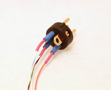
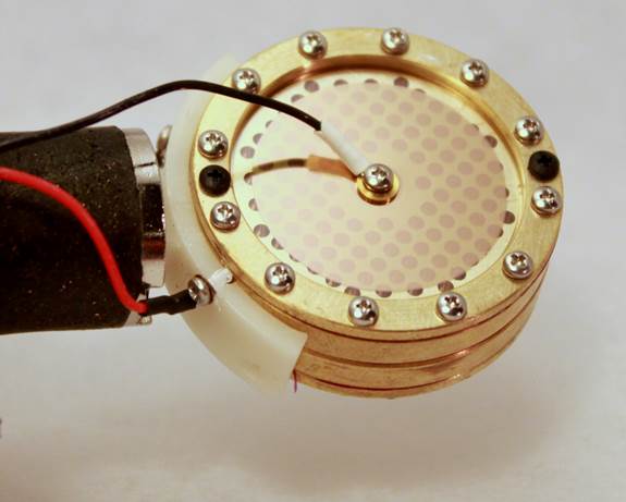
K87-style capsule with four leads — front diaphragm, front backplate, rear diaphragm, rear backplate. Short but relaxed wires.
Gloves on throughout. Handle the capsule by the outer rim only — never touch the diaphragm.
Verify backplate isolation before wiring: DMM Ω between the two backplate terminals must read open circuit.
Multi-pattern (K87 isolated-backplate): wire all four terminals — FD, FBK, RD, RBK.
Cardioid-only (K67 / shared-backplate): wire only FD and FBK; leave RD and RBK unconnected.
Mount into saddle gently — do NOT overtighten. Keep wires short but relaxed.
⚠️ Most delicate step of the entire build
The diaphragm is sensitive to finger oils, dust, flux residue, and contact. Gloves on throughout — no exceptions.
⚠️ Verify backplate isolation after mounting
Mount stress can shift a backplate enough to short to the other — particularly on Peluso PK87i with an over-tightened central screw. Check isolation again after installation.
13
Body Assembly & First Test
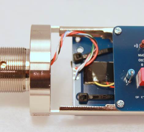
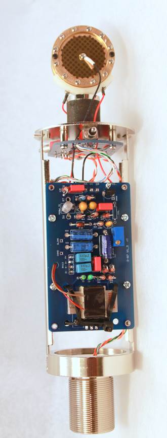
Assembly complete — PCB stack, transformer, and capsule in position before the sleeve and headbasket close the body.
Insert calibrated PCB assembly into the body. Align switches against the cutouts. Secure with M2 × 4 mm screws — firm, not torqued.
Install sleeve and headbasket. Tighten threaded sections to firm contact only.
First test: connect to preamp, gain low, phantom on. Increase gain to normal speaking level. Expected: 45–55 dB of preamp gain — this is a design characteristic, not a fault.
Cycle through polar patterns (mute monitors before each switch). Verify all three patterns produce output.
Confirm self-noise is acceptable. Hum that disappears when touching the body chassis = Faraday-cage failure.
⚠️ Faraday-cage continuity check
With body assembled and XLR connected, verify continuity from XLR pin 1 to every metal part (headbasket, sleeve, end cap, rails). More than a few ohms at any path = paint, anodizing, or oxidation at that seam. Sand the contact surface.
▶ 💡 Storage
The wooden storage box accepts the assembled mic and shock mount together. Store when not in use — dust and moisture both degrade self-noise over time.
Stuck?
45+ questions — 14 years of builds, distilled
Before posting on the forum, search here first. These answers were extracted from 14 years of community discussion — the most common problems, solved.
🔍
No matching questions — try a different search term or clear the filter.
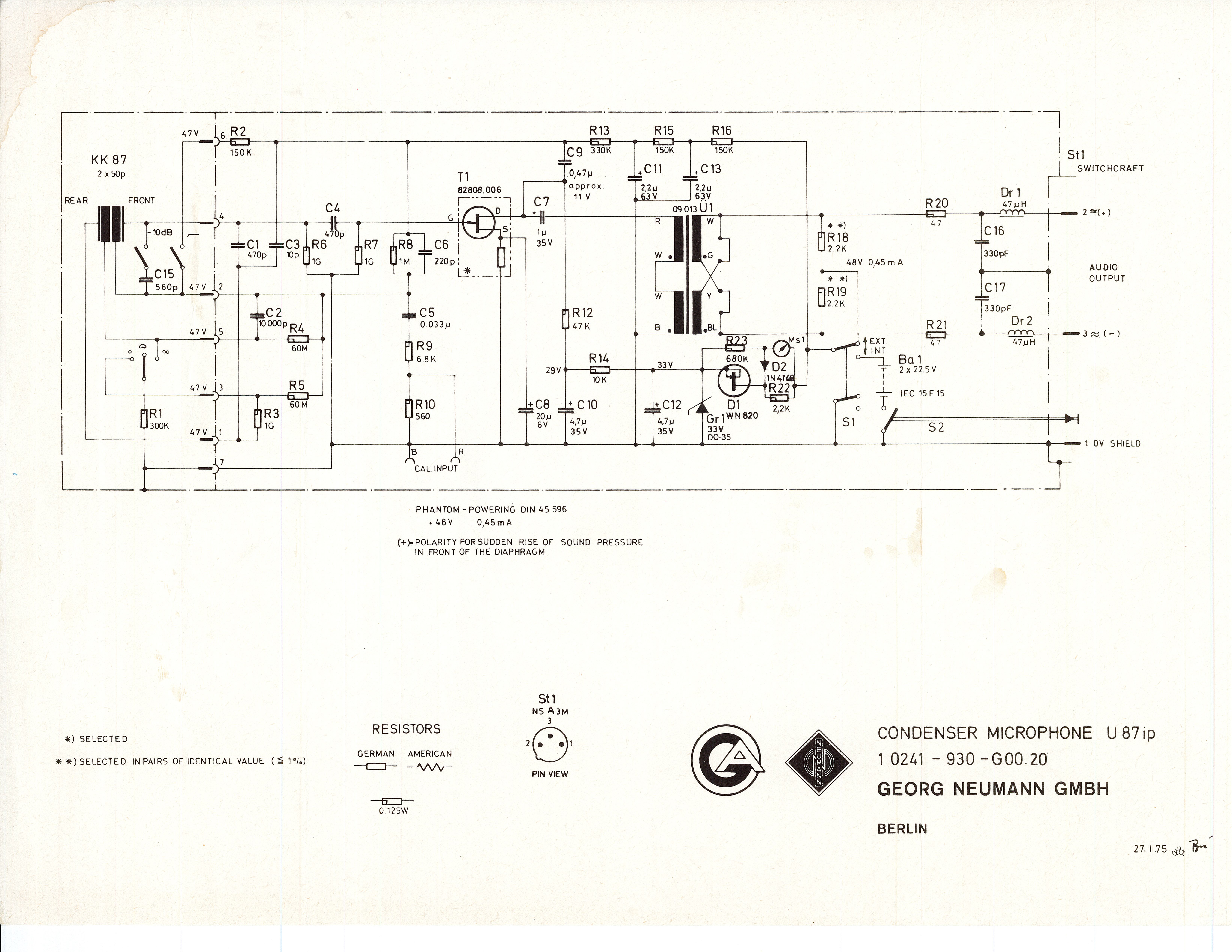
Circuit Reference
Click to enlarge · Neumann U-87 reference schematic
Key nodes: FBK = capsule front-backplate polarization (~40 V design, ~17 V measured by DMM — see FAQ); drain target = 10.5 V DC; Zener = 24 V ±5 %; phantom = 48 V at top of L1/L2.
Component List
33 line items · 40 components · rev 1R0a
#
Ref
Qty
Value
Description
Part Number
Type
Errata
Known issues — read before you build
ID
Severity
Affects
Description
E1
Critical
Green PCB only
R6 must be installed reversed. On the Green PCB (D-87L), install R6 (1 GΩ, TE Connectivity RGP0207CHK1G0) reversed relative to the silkscreen orientation. This exposes one lead for the C4-R6 junction biasing technique. Blue PCB does NOT require reversal.
E3
Critical
All variants
PCB silk labels do not match XLR pin numbers. Mapping: PCB "1" → XLR pin 2 (Hot); PCB "2" → XLR pin 3 (Cold); PCB "3" → XLR pin 1 (GND). Wiring 1:1 from the silkscreen produces a polarity swap or grounding fault.
E4
Critical
AMI T13 transformer
AMI / TAB-Funkenwerk T13 color code is reversed for the U-87 application. Black wires = primary (~440 Ω, capsule side, RT/SW pads). Yellow wires = secondary (~22 Ω, XLR side, WS/BL pads). Always DCR-test before soldering. AMI has not corrected their documentation as of 2026.
E5
Critical
Green PCB V1.1 / V1.2 only
R12 / R13 silkscreen designators are visually ambiguous. R12 = 47 kΩ; R13 = 330 kΩ. Swapping them places the drain at ~1 V regardless of trim pot setting. Verify against the corrected reference image before soldering.
E6
Critical
NTE312 substitution only
NTE312 pinout differs from 2N3819. Gate is on an outer pin, not the center. Install NTE312 rotated 180° from the silkscreen orientation. Installing in 2N3819 orientation produces a non-functional bias state and damages the FET.
E2
Warning
Green PCB only
Capsule connection board polarity marking. On some Green PCB revisions the FD / RD silkscreen labels on the capsule connection board are mirrored relative to the main board wiring convention. Verify wiring against the capsule step in this guide before soldering.
Ready to build?
The complete kit — PCB, matched components, StyroFlex caps — is available at microphonediy.com.